Posted on Leave a comment

Repairing a Switch Power Supply Fault in a TECO 7200GA-30kW Inverter: A Detailed Diagnostic and Solution Guide

In the realm of industrial machinery, inverters play a crucial role in converting direct current (DC) to alternating current (AC), enabling the efficient operation of various electrical devices. However, like any complex electronic system, they are susceptible to faults, especially after encountering events such as lightning strikes. This article delves into the diagnostic process and subsequent repair of a TECO 7200GA-30kW inverter that exhibited random shutdowns and starting difficulties following a lightning-related repair.
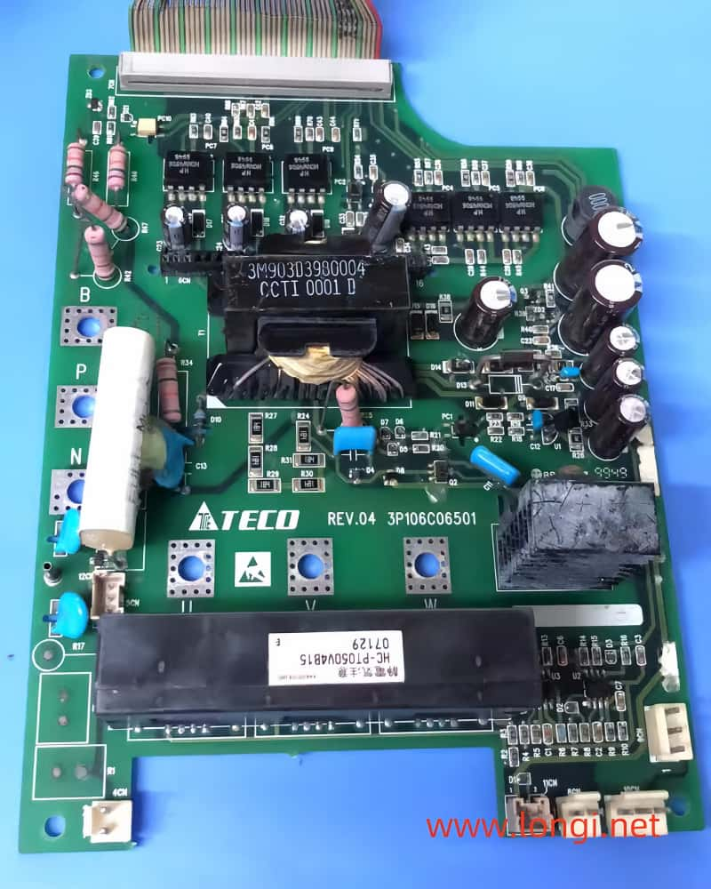
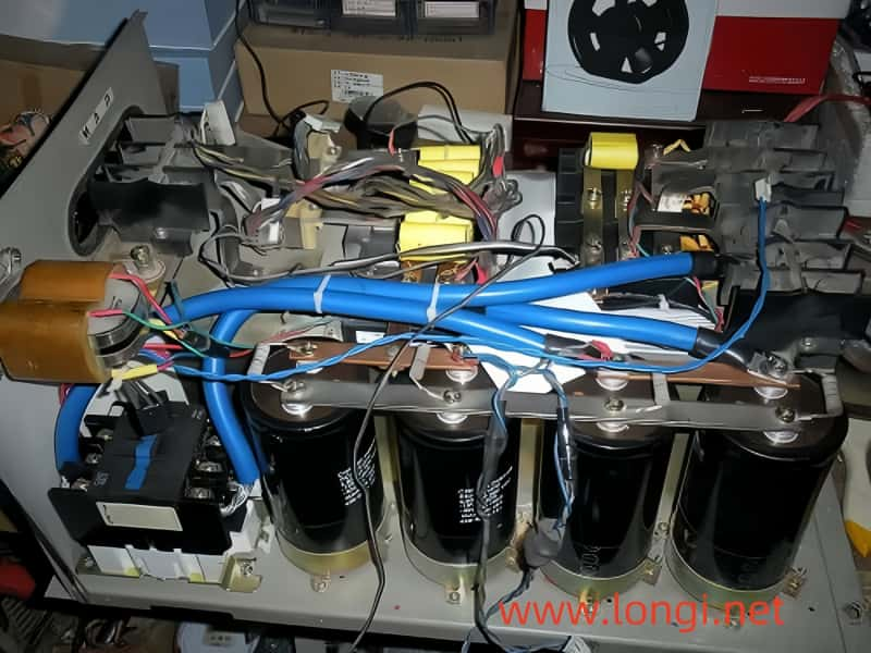
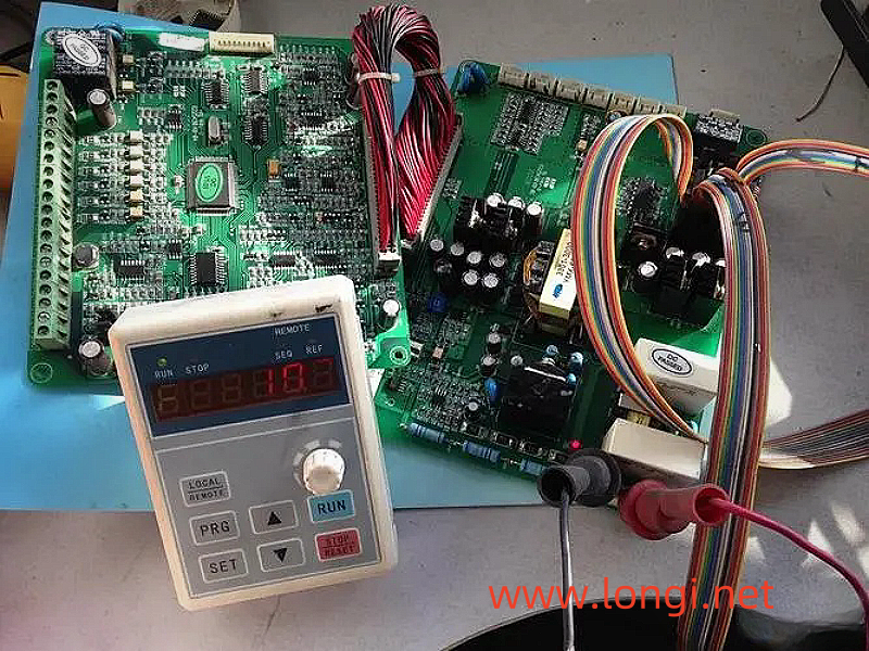
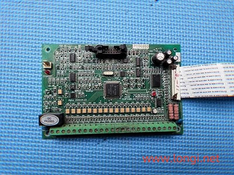
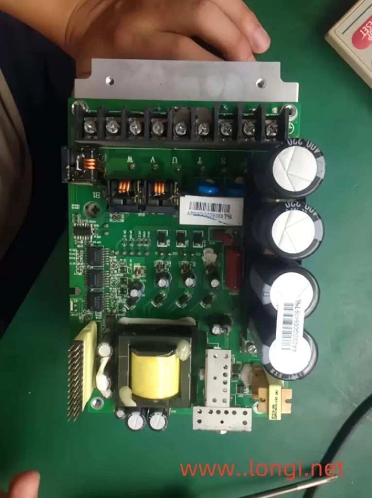
TECO INVERTER power board

Initial Symptoms and Preliminary Inspections

The inverter, after being repaired from lightning damage, operated inconsistently for over a month. It experienced random shutdowns, sometimes occurring every few days or hours, and encountered difficulties during the starting process. Specifically, the capacitor charging short circuit contactor would jump, leading to failed starts, yet the operation panel did not display any fault codes. Despite these challenges, the inverter could occasionally start and run for a period before shutting down again.

To begin the diagnostic process, the control board was removed from the site. To bypass potential thermal protection issues, the terminals of the thermal relay were short-circuited. Similarly, the contact detection terminal of the capacitor charging contactor was short-circuited to prevent low voltage protection states. However, these measures did not resolve the issue, prompting a more comprehensive inspection. Upon detailed examination, no visible abnormalities were found, indicating that the problem was likely more complex and required a deeper investigation.

Identifying the Root Cause

With the control board reinstalled, testing revealed that the contactor jumped during startup, preventing the inverter from initiating. Interestingly, unplugging the 12CN plug cooling fan significantly improved the starting success rate. Observing the display panel during startup showed a decrease in brightness, suggesting a problem with the control power supply’s load capacity.

Further testing under load conditions revealed that while the power supply outputs were normal when unloaded, connecting resistive loads caused voltage drops. Specifically, when a 24V load was connected to the cooling fan and relay, the +5V line dropped to +4.7V. Although the screen display and other operations remained normal at this voltage, attempting to start the inverter resulted in the relay jumping and occasional fault codes such as “low DC voltage” and “communication interruption between CPU and operation panel.” Measurements indicated that when the +5V dropped below +4.5V, the inverter would automatically switch from the starting state to standby mode.

Analysis and Solution

The diagnosis of poor load capacity in the control power supply was confirmed. The CPU, with its strict power supply requirements, could barely function at voltages no less than 4.7V but would enter standby mode at voltages below 4.5V. The challenge lay in the fact that despite thorough checks, no components of the switch power supply were found to be damaged.

In an attempt to adjust the output voltage, a parallel resistance test was conducted on R1, one of the reference voltage divider resistors of the U1 (KA431AZ) voltage regulator. While this slightly increased the output voltage, the load capacity remained insufficient. Closer inspection of the circuit board revealed welding marks on the diversion adjustment tube Q1, indicating potential previous modifications. However, replacing Q1 with a similar component from another machine did not resolve the issue.

Given the complexity of the circuit and the high specificity of the transistors involved, particularly the bipolar transistor Q2 with high back pressure and amplification, a more nuanced approach was required. Analysis suggested that the working point of the shunt adjustment tube Q1 had shifted, causing excessive shunting of the base current of Q2. This, in turn, compromised the power supply’s load capacity.

To address this, a resistor (R6, 330 ohms) was series-connected with a voltage feedback optocoupler and a 47-ohm resistor. This modification aimed to reduce the base current of Q1, thereby decreasing its shunting capability towards Q2 and enhancing the power supply’s load capacity. Upon testing, the +5V line stably maintained 5V output, both under load and during startup operations, effectively resolving the issue.
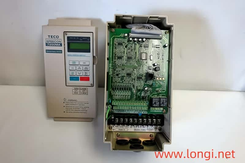
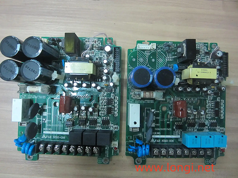
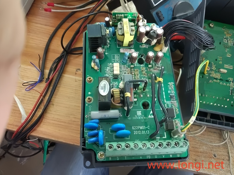
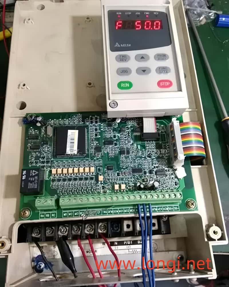
TECO inverter 7200

Fault Inference and Conclusion

The fault was inferred to be due to the aging of the Q1 switch tube, leading to a decrease in its amplification ability. This resulted in insufficient base current (Ib) after shunting, causing Q1 to become fully conductive and increasing its conduction resistance. Additionally, a characteristic deviation in the shunt branch led to excessive shunting and poor driving of the switching tube, further reducing the power supply’s load capacity.

In summary, the repair process of the TECO 7200GA-30kW inverter involved meticulous diagnostic steps, from initial symptom observation to component testing and eventual circuit modification. The successful resolution highlights the importance of understanding the intricate workings of electronic systems and the creative application of engineering principles to overcome unexpected challenges. This case study serves as a valuable resource for technicians and engineers facing similar issues in industrial electronics repair.

Posted on Leave a comment

Troubleshooting and Repairing a Switch Power Supply Malfunction in the Jialing VSD JP6C-9 Model

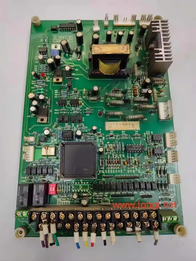
When dealing with complex electronic devices like the Jialing VSD JP6C-9, encountering issues such as a malfunctioning switch power supply can be both frustrating and challenging. This article details a step-by-step diagnostic and repair process for a specific case where the operation panel failed to display any information upon powering on, despite the input and output terminals of the main circuit exhibiting normal resistance levels. The root cause was identified as a power failure on the control board switch, accompanied by tell-tale signs of an abnormal power load.

Initial Observations and Symptom Analysis

Upon initial inspection, the most glaring symptom was the complete lack of display on the operation panel. Given that the resistance checks on the main circuit’s terminals were within acceptable ranges, it became evident that the issue was not with the primary power delivery but rather with the control circuitry. The presence of intermittent clicking sounds, which indicated a struggle in initiating the power supply, further narrowed down the potential culprits. Based on experience, such sounds often suggest issues related to power load abnormalities.

Systematic Diagnosis

The first step in the diagnostic process involved examining the rectification, filtering, and load circuits of each power supply segment. These components are crucial in ensuring smooth and stable power delivery. After thorough checks, no irregularities were found in these circuits, ruling out common failure points.

Next, an attempt was made to isolate and disconnect high-current power supply branches, including the cooling fan power supply, inverter drive power supply, and operation panel display power supply. This isolation technique is often effective in pinpointing which branch might be causing the overload. However, even after disconnecting these branches, the problem persisted, indicating that the issue was more deeply ingrained within the core power supply circuitry.

Deep Dive into the Switch Transformer Circuit

With the basic circuits ruled out, attention turned to the more intricate components of the power supply, specifically the peak voltage absorption network associated with the primary winding of the switch transformer. This network, typically comprising a resistor and capacitor in parallel, connected in series with a diode, serves a critical role in protecting the switching tube from abnormal peak voltages during its cut-off period.

Using a pointer multimeter, the forward and reverse resistance of the diode was measured, revealing an unusual reading of 15 ohms in both directions. This anomaly prompted a closer examination of the diode itself. Upon disassembly and individual testing, the diodes were found to be functional, suggesting that the issue lay elsewhere in the network.

A meticulous visual inspection revealed subtle cracks in the capacitor within the peak voltage absorption network. Further testing confirmed that the capacitor, rated at 2kV 103, had indeed suffered a breakdown and short-circuited. This discovery was crucial, as the capacitor’s failure had significant implications on the operation of the switch transformer.

Understanding the Impact of the Capacitor Failure

In a properly functioning system, the peak voltage absorption network absorbs energy during the switching tube’s conduction period, which is then safely discharged through the diode during the tube’s cut-off period. This mechanism prevents excessive voltage spikes from damaging the switching tube. However, with the capacitor short-circuited, the primary winding of the switch transformer was effectively paralleled with the diode. As a result, the energy accumulated during the conduction period was rapidly discharged, preventing the necessary oscillation energy from being stored.

Moreover, the diode acted as an excessive load on the switch transformer, impeding its ability to initiate the power supply’s startup sequence. This unusual manifestation of a capacitor short-circuit causing startup difficulties is relatively rare and underscores the importance of meticulous component inspection in troubleshooting such issues.

Repair and Restoration

With the faulty capacitor identified, the repair process involved replacing it with a new one of the same specifications. After the replacement, the machine was powered on once again, and this time, the operation panel lit up as expected, indicating a successful repair. The switch power supply was now functioning correctly, free from the previous startup difficulties.

Conclusion

This case study highlights the intricacies involved in diagnosing and repairing switch power supply malfunctions, particularly in sophisticated devices like the Jialing VSD JP6C-9. It underscores the importance of a systematic approach, thorough component inspection, and the use of appropriate diagnostic tools. By understanding the functionality of each component and its role in the overall system, technicians can effectively pinpoint and resolve even the most perplexing issues, ensuring the reliable operation of electronic equipment.

Posted on Leave a comment

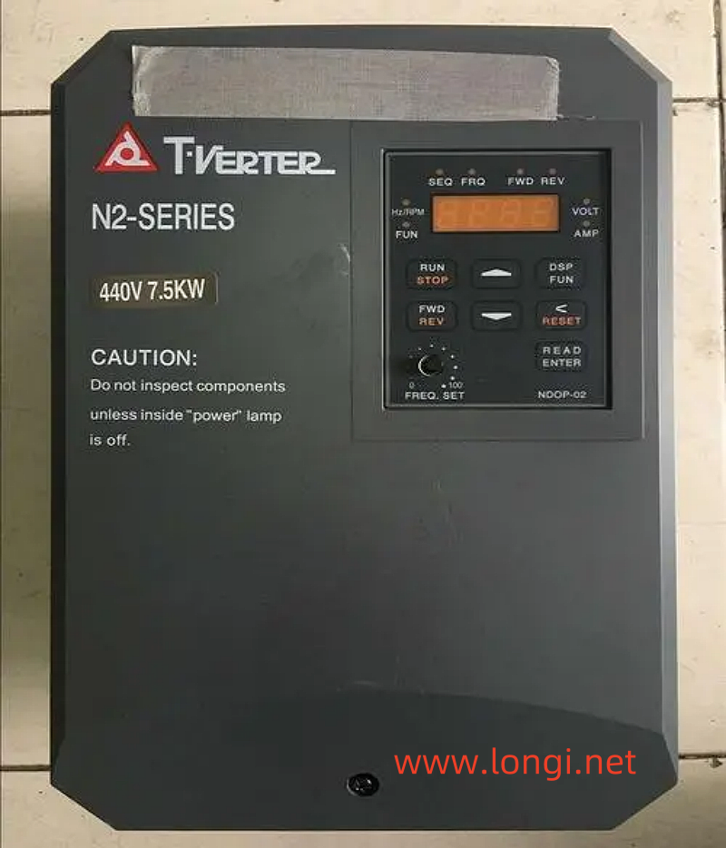
Maintenance of Switch Power Supply Fault in Taian N2-1013 VSD

Upon powering on, there was an OC fault. It was detected that the inverter output module was not damaged, and most of the six inverter drive ICs were damaged. Further inspection revealed a peculiar phenomenon in the switch mode power supply: when the CPU motherboard was disconnected for power supply,+5V was measured to be normal, but the power supply of other branches was higher than normal, such as+15V being+18V, and the driving power supply of 22V being 26V. When the wiring block of the CPU motherboard was connected,+5V was measured to be normal, but the power supply of other branches showed an abnormal increase! If the driving power supply of 22V even rises to nearly 40V (the maximum supply voltage of PC923 and PC929 is 36V), the damage to the driving IC is caused by this.

Key inspections were conducted on the voltage stabilization process, and peripheral circuits such as IC202 and PC9 showed no abnormalities. Further investigation revealed no abnormalities in other circuits, and maintenance was deadlocked.
Analysis: The voltage stabilizing part of the circuit works. The voltage sampling of the voltage regulator circuit is taken from the+5V circuit. When the wiring block of the CPU motherboard is unplugged, it is equivalent to a light load or no load of+5V. The rising trend of+5V increases the negative feedback of the voltage, reduces the duty cycle of the power switch driver pulse, reduces the excitation current of the switch transformer, and the output voltage of other branches is relatively low; When inserted into the wiring block of the CPU motherboard, it is equivalent to a+5V load or overload. The decreasing trend of+5V reduces the negative voltage feedback, increases the duty cycle of the power switch driver pulse, and increases the excitation current of the switch transformer, causing the output voltage amplitude of other branches to increase. The current situation is that when the+5V circuit is unloaded, although the output of other power supplies is lower, it is still higher+ After 5V loading, other power supply branches exhibit abnormally high voltage output! The faulty link is either due to a malfunction of the power supply itself causing a decrease in load capacity, or an abnormality in the load circuit. Both abnormalities have caused the voltage regulator circuit to undergo conscientious “misregulation”, resulting in the maintenance of the “voltage stability” of the+5V faulty circuit and the occurrence of “abnormal voltage changes” in other power supply branches!

Start repairing the+5V circuit, unplug the power filter capacitor C239220u10V, and check that the capacity is only a dozen microfarads, with obvious leakage resistance. The failure of a capacitor perfectly satisfies two conditions: a decrease in capacity reduces the power supply’s carrying capacity, and leakage causes the load to become heavier.
After replacing this capacitor, the test run was normal.

Posted on Leave a comment

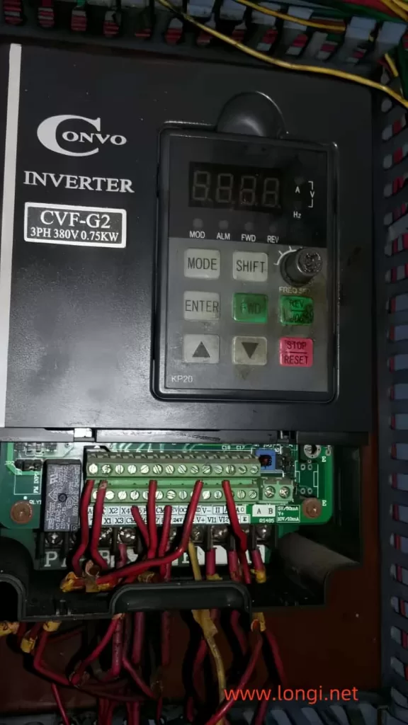
Troubleshooting Guide for CVF-G1 Switching Power Supplies in CONVO Frequency Converters

Title: Troubleshooting Guide for CVF-G1 Switching Power Supplies in CONVO Frequency Converters

Introduction:
We recently received three CVF-G1 frequency converters from Kangwo, all exhibiting identical issues: no output from the switching power supply and no screen display. Given that the power supply IC in these machines is a 3844B, and considering the rarity of this IC causing failures in multiple units simultaneously, we embarked on a troubleshooting journey focusing on the peripheral circuits.

Understanding the Switching Power Supply:
A typical switch-mode power supply comprises several key branches:

  1. Power-On Start Branch: This consists of a series of high-resistance resistors that, upon powering on, direct 500V DC to the 3844B power supply pin, initiating the switch tube’s starting voltage.
  2. Positive Feedback and Working Power Supply Branches: These are composed of feedback windings and rectifier filtering circuits, varying between machines in configuration.
  3. Voltage Stabilizing Branch: Powered by a secondary 5V supply, this branch compares 5V voltage changes against a reference, feeding back variables to the 3844B via an optocoupler. Notably, the CVF-G1 model feedback is derived from the primary side.

Conditions for Circuit Oscillation:
For the circuit to oscillate, the following must be met:

  1. The 500V power supply circuit must be functional, delivering DC voltage to the switch’s drain through the main winding.
  2. The power-on start branch must supply an adequate starting voltage (current).
  3. The positive feedback and working power supply branches must provide the necessary feedback voltage (current) and working power.
  4. The load side must be free of short circuits, as these prevent the establishment of sufficient feedback voltage, halting oscillation.

Troubleshooting Approach:
To pinpoint the fault, we began by isolating the voltage stabilizing branch to check if the circuit could oscillate without it. We ensured safety by implementing voltage reduction and disconnecting circuits susceptible to voltage damage. If the circuit oscillated, it suggested that the oscillation conditions were generally met, shifting our focus to the voltage stabilizing branch for further investigation. If not, the issue lay within the oscillation circuit itself.

Findings and Repairs:

  • Machine A: All four branches and 3844B peripherals checked out normal. Replacing the 3844B with a 3845B restored power output.
  • Machine B: Despite replacing the IC with a 3845B, oscillation failed to initiate. All branch components appeared normal. However, paralleling a 200k resistor with the existing 300k resistor in the power-on start branch resolved the issue, indicating a subtle performance shift in one or more components affecting electrical parameters.
  • Machine C: The fault was traced to the 3844B IC, and replacing it resolved the issue.

Analysis of Machine B’s Unique Fault:
Machine B’s fault was particularly intriguing. No obvious defective parts were found, yet it failed to oscillate until the starting branch’s resistance was adjusted. This suggests minor changes in component performance, such as reduced switching tube amplification, moisture-affected transformer Q values, increased 3844B output resistance, or slight variations in resistance/capacitance components. Identifying these precise causes can be challenging, but they all lead to one outcome: ineffective switch tube activation. Adjusting the starting branch’s resistance proved to be an effective solution, highlighting the importance of adequate starting current for circuit oscillation.

Conclusion and Recommendations:
Based on our experience, an efficient repair strategy for similar issues involves:

  1. Verifying the switch tube’s integrity and the general functionality of the four branches.
  2. Conducting a parallel resistance test on the starting branch.
  3. If unsuccessful, replacing the 3844B IC.
  4. If issues persist, conducting a thorough circuit inspection.

Often, issues are resolved during the initial tests, emphasizing the importance of a systematic approach to troubleshooting. Additionally, considering the role of starting current in circuit oscillation, adjusting the starting branch’s resistance may offer a simple yet effective solution in many cases.

Posted on Leave a comment

Repair Guide for INVT G9 Series Frequency Converter “Crash” Fault

Repair Guide for INVT G9 Series Frequency Converter “Crash” Fault

When dealing with a reported “crash” fault in an INVT G9 series frequency converter, a systematic approach to diagnosis and repair is crucial. This article outlines a step-by-step process based on user feedback, detailed inspection, and successful repair.

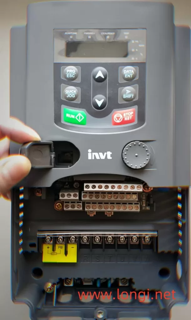
INVT INVERTER physical picture

User Feedback and Initial Observations

The user reported that the frequency converter was not operational at the time of the incident, but other machines on the same three-phase power supply experienced abnormalities, leading to a short circuit and tripping. Consequently, the power switch for the frequency converter also tripped. Upon attempting to reset the power switch, it was discovered that the operation panel was no longer displaying any information, prompting the need for repair.

Detailed Inspection and Fault Identification

Upon inspecting the frequency converter, an open circuit was found between the R, S, T terminals and the main DC circuit (P and N). Further disassembly revealed that the copper foil strip connecting to the module had been damaged by an arc. Testing confirmed a short circuit at the three-phase power supply terminal of the module.

Root Cause Analysis

The root cause of the malfunction was traced back to instantaneous short circuits and tripping of other load branches in the power supply, which induced abnormal voltage spikes in the three-phase power supply. These dangerous voltage levels caused the rectifier circuit in the frequency converter module to break down and short circuit. The resulting strong arc burned the copper foil strip and triggered the power switch to trip.

Repair Plan

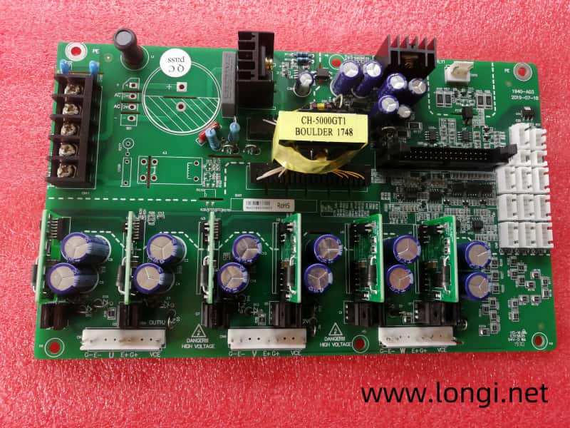
INVT inverter drive board

Fortunately, the inverter part of the module was still functional, with no signs of bulging or deformation. Therefore, the decision was made to cut off the damaged rectification part of the module and install an additional three-phase rectification bridge. This low-cost repair plan allowed for the reuse of the original three-phase inverter circuit in the module.

Inspection and Troubleshooting

To prevent further abnormalities, the power supply to the inverter section of the module was cut off. A 500V DC voltage was applied from an external repair power supply, but the operation panel displayed “H.00,” and all operations were ineffective. Based on experience, this indicated that the module’s short circuit detection function had activated, causing the CPU to reject all operations.

Further inspection revealed that the overcurrent signals in the fault signal collection and processing circuit were all negative, whereas they should have been positive under normal conditions. Tracing the current detection circuit, it was found that an incorrect overcurrent signal was being output. By disconnecting the overcurrent fault signal, the operation panel’s parameter settings returned to normal, but the start/stop operation still had no response.

Additional Fault Signals and Resolution

Suspecting that there might be other fault signals causing the frequency converter to remain in protection mode, the voltage at the module’s thermal alarm terminal was measured and found to be 3V, lower than the normal 5V. It was hypothesized that the damaged rectification circuit might be outputting a thermal alarm signal. By cutting off the copper foil strip connected to the thermal alarm, the start/stop operation on the operation panel became effective.

Protection Sequence and Final Repairs

The protection sequence of the INVT G9/P9 frequency converter is designed to ensure safe operation. If a fault is detected in the power inverter output section during power-on detection, the SC – output short circuit fault code will be displayed, and all operations will be rejected. Similarly, if an overcurrent signal is detected, “H.00” will be displayed, and all operations will be halted. When a thermal alarm signal is detected, most operations can be performed, but the startup operation is rejected to prevent overheating.

To complete the repair, the damaged copper foil strip lead of the three-phase power supply was cut off, cleaned, and properly insulated. An external three-phase rectifier circuit was connected, and its DC output was introduced to the P and N terminals. Additionally, a thermal protection circuit was installed using a 60℃ normally closed thermal relay, which is connected in series with an NPN type transistor base to the 5V ground circuit. This ensures that the module does not overheat and burn, providing an additional layer of safety.

By following this structured approach, the INVT G9 series frequency converter was successfully repaired, restoring it to full functionality.

Posted on Leave a comment

Handling Method for SC Jumping Fault of GS Series INVT VSD

SC: Refers to a short circuit in the output load of the frequency converter. In the state of power outage, there is no short circuit between U, V, W and between U, V, W and DC P, N. To distinguish whether it is a current detection circuit fault on the CPU motherboard or a signal returned by the driving IC, short circuit the signal to the diode side of the optocoupler device with a wire, and operate the RUN key after power on. The output frequency displayed on the panel is normal. The SC signal is returned by the driving IC, and there are two reasons for the malfunction: first, the inverter module is damaged, and second, the driving IC itself is faulty.

After cutting off the power supply to the inverter module, the six pulse signals of the drive IC were checked again. It was found that the U-upper arm drive IC had input pulses but no output pulses (static negative pressure normal). After replacing the drive IC, the output was normal. The static negative pressure of the U lower arm drive IC is only a few tenths of a volt. After replacement, the fault still persists. After welding the 100 ohm resistor connected to the trigger end of the inverter module, the static negative pressure rises to the normal value. The forward resistance of the lower arm terminal of the module U is consistent with the resistance of other trigger terminals, but its reverse resistance is slightly smaller than that of other trigger terminals, indicating that the circuit inside the U-phase trigger terminal of the module is damaged!
This is a key point in checking module faults: the resistance of the main terminal cannot be roughly measured to be normal, which means that the module is good. It is not uncommon for the circuit inside the triggering terminal to be damaged, but it is more concealed! When the frequency converter reports an SC or OC fault and the main terminal of the detection module is normal, the inspection of the forward and reverse resistance of the triggering terminal should not be missed!
The damage of modules and the damage of driving ICs are usually related: when the U-phase main circuit is damaged, the upper and lower arm driving ICs of the U-phase are often also damaged by strong voltage shocks; When the driver IC of the phase is found to be damaged, it often hides the internal circuit damage of the triggering terminal of the phase. So one of the two is that a comprehensive inspection must be conducted. Of course, there are also cases where modules and driver ICs are damaged separately, but it is extremely rare.

During maintenance, another phenomenon of drive IC failure was also discovered in the low-power model of the Envision GS: when the frequency converter is powered on and there is an SC fault signal output, the CPU performs self check, reset, and reset, and after clearing, the panel only displays H:00, and all panel buttons fail to operate. When the corresponding optocoupler circuit is short circuited to eliminate the SC signal, all panel operations are normal. If the model detects an SC fault signal output when powered on, it may perform a “program lock” and refuse to operate! When this phenomenon occurs, the fault signal output circuit should be checked and corresponding measures should be taken to temporarily eliminate the fault signal, in order to facilitate operation and judgment, and thus solve the fault.

Posted on Leave a comment

Special situation of Alpha VFD tripping OC fault

Generally speaking, there are two sources of OC faults:

  1. When the operating current of the inverter module is too high, reaching more than three times the rated current, and the voltage drop of the IGBT tube rises to more than 7V, the driving IC returns an overload OC signal to notify the CPU and implement fast shutdown protection;
  2. After collecting a sharp increase in abnormal current from three current transformers at the output end of the frequency converter (some low-power models use two), a voltage comparator (or internal circuit of the CPU) outputs an OC signal to notify the CPU and implement fast shutdown protection.

Of course, when the driving IC or current sampling circuit is abnormal, the frequency converter will falsely report an OC fault.
Small power models often use a shunt resistor directly connected in series at the output end to collect current signals. After being amplified in the front stage, they are isolated by an optocoupler operational amplifier and transmitted to the CPU. The power supply of its preamplifier is taken from the floating power supply of the driving IC. In this way, when the module is damaged (or removed), the power supply branch connected to the inverter module is broken, causing the current sampling circuit to output the highest negative pressure. The CPU mistakenly believes that there is a large current signal and reports an OC fault. In this situation, the frequency converter trips the OC fault as soon as it is powered on, making it impossible to inspect whether the drive IC circuit can output six normal trigger pulses.
In addition, if the peripheral circuit of the driving IC is abnormal or damaged, it can also misreport OC faults. Therefore, during maintenance, it is necessary to distinguish whether it is a fault reported by the current sampling circuit or the driving IC, whether it is a circuit damage misreport or a module damage. Is there really an overcurrent fault? And take measures to clear the alarm status for easy maintenance.
But the OC jumping faults caused by the following reasons often go unnoticed. Overhaul an Alpha frequency converter. Due to damage to the main DC circuit voltage detection circuit, the voltage on terminal 8 was 0 (normally around 3V). The frequency converter experienced an undervoltage fault and could not be put into operation. When the terminal is artificially fed with a voltage of+5V, the frequency converter trips the OC fault when powered on. Through experiments, it has been proven that when the voltage is below 2.5V, an undervoltage fault code will trip, and when the voltage is above 3.8V, an OC fault will trip. Therefore, it is found that when the DC circuit voltage is too high or the DC detection circuit is abnormal, it is another reason for the frequency converter to trip the OC fault.

When conducting maintenance or emergency response, take 5V voltage from the 8 pins of the wiring block CN1 and fix a 3V voltage with a divider resistor. This will facilitate maintenance or emergency operation of the frequency converter.

Posted on Leave a comment

A Hidden Cause of Alpha Inverter OC Fault Tripping and Shutdown

During the maintenance of the Alpha low-power inverter, it was discovered that the inverter has a common problem – it is prone to OC failure. It manifests as: often jumping faults during start and stop operations, but sometimes also jumping faults during operation; Sometimes it inexplicably improves and can run for varying lengths of time. When I thought there was no problem, I started to frequently skip OC faults again; When measuring the output voltage of U, V, and W with a probe under no load, it is prone to tripping faults. However, after connecting the motor, it starts running and does not jump again. After a while, the OC fault still jumps when connecting the motor.

The handling of such faults is quite tricky, and it is possible that the fault has been eliminated during the testing process, resulting in no evidence for investigation. Even when testing the hardware circuit (protection circuit) during frequent malfunctions, I couldn’t find any problems and couldn’t figure out the root cause of the problem. This problem puzzled me for over two months.
The hardware protection circuit is mainly completed by two LM393 dual operational amplifier circuits, U22 and U24. The signal is then inverted by a first stage inverter and sent to pin 16 of the CPU. U22 and U24 jointly input two output current signals, one overload OC signal returned by the inverter drive IC, and one DC voltage detection signal, which are respectively added to the input terminals of four operational amplifiers. After open-loop amplification processing (the operational amplifier circuit is actually used as a switch circuit here), Four fault signals were connected in parallel, and after undergoing a first level of phase inversion processing, they were sent to pin 16 of the CPU. I first cut off the overload OC signal returned by the inverter drive IC, and then cut off the “total” fault signal of the inverter output, but both were ineffective, and the fault phenomenon still persists. Is there another way to string in OC signals elsewhere? Impossible!
There may be some inexplicable interference in the circuit, but the source and cause of the interference are difficult to identify. We racked our brains and exhausted all means to install capacitor and resistor filtering elements in the fault signal circuit to improve the anti-interference performance of the circuit, but to no avail. Could it be that during the loading and unloading process of the inverter drive module during the start/stop moment, the fluctuation of CPU power supply caused the malfunction? The measured CPU power supply is 4.98V, which is very stable and meets the requirements.
Without any reason, I had a sudden inspiration and adjusted 4.98V to 5.02V. After conducting a start/stop test, the fault was surprisingly eliminated!
Analyze and speculate the cause of the malfunction as follows: the setting of the static voltage working point outside or inside the CPU is improper or too low, which is exactly at the critical point of signal interference level, making it easy to experience random OC faults that are confusing. After slightly increasing its 5V power supply, the voltage value at its operating point also increases accordingly, avoiding the critical point of interference level, and the frequency converter changes from “neural” to “normal”.

When the machine leaves the factory, if the CPU power supply adjustment value is slightly higher, the machine can run normally for a long time. If the adjustment value is slightly lower, or if there is a slight decrease in 5V due to some reason (such as component variation, temperature drift, etc.) during use, frequent OC tripping faults may occur. Adjusting the 5V power supply can easily solve the problem while ensuring that there are no issues with the hardware protection circuit. If it is not due to an accidental factor, then the depth of the concealment of this fault makes it difficult to “adjust” it properly.

Posted on Leave a comment

Repairing Two Delta VFD-A Frequency Converters: A Detailed Guide

In the realm of industrial equipment maintenance, frequency converters play a crucial role in controlling motor speed and efficiency. Recently, I encountered two Delta VFD-A frequency converters that required extensive repairs due to severe damage in their output modules and driving circuits. This article documents the step-by-step process of diagnosing, repairing, and testing these converters, highlighting key lessons learned.

Initial Inspection and Diagnosis

Upon receiving the two converters, a thorough inspection revealed significant damage: the output modules were compromised, and the driving circuits were in poor condition. Specifically, the T250V driving integrated circuits were either exploded or short-circuited to the power supply ground. Additionally, filtering capacitors had leaked, voltage regulator tubes were broken, resistors were open or had increased resistance, and the circuit boards were carbonized.

Further inspection of one converter revealed a broken arm in the three-phase rectifier bridge, along with a damaged charging current limiting resistor. The charging resistor was short-circuited, and the relay contacts were stuck, leading to severe damage. Several signal introduction resistors on the input side of the driving integrated circuit were also open, indicating that the CPU had likely suffered a strong electrical shock.

Circuit Analysis and Component Replacement

With the main circuit and driver circuit diagrams in hand, I began a comprehensive inspection. Using a small knife, I scraped off the carbonized parts of the circuit board and removed all damaged components. After ensuring there were no short circuits in the main circuit, I powered on the converter for a preliminary inspection. The display was normal, indicating that the switch power supply and control section were functioning.

An oscilloscope measurement of the six driver inputs (trigger signals from the CPU) revealed a peak voltage of 1.5V and a carrier frequency of 10kHz, which varied with frequency and pulse width. This confirmed that, apart from the damaged inverter and drive circuits, all other circuits were operational. The CPU’s three-phase pulse output terminal had withstood the electrical shock remarkably well.

I immediately procured the necessary replacement parts and began the repair process. Over 30 components in the driver circuit were replaced, and I tested the static DC voltage of each pin of the driver integrated circuit upon powering on. All measurements were within normal ranges. An oscilloscope was then used to measure the output waveforms of each integrated circuit, which were also within normal limits. With these repairs complete, I proceeded to weld the inverter output module.

Testing and Further Issues

Upon powering on the repaired converter for testing, I noticed a three-phase imbalance using a multimeter. Switching to the DC 500V range revealed no DC component between V and W, but there was DC voltage between U and V, as well as U and W. This indicated an issue with the U-phase output.

Further inspection revealed that the voltage regulator diode DD11 in the EU circuit’s triggered power supply was damaged. After replacing it with a regular component (the original SMD component had weak bonding), I accidentally desoldered it during the installation of the inverter module. This caused the triggering end of the upper transistor in the U-phase to be forced to a low level, resulting in only the negative half-wave output of the lower transistor being conductive.

I re-soldered DD11 and tested the machine again. The three-phase output was balanced, and there was no DC component. A 5.5kW submersible pump was connected for further testing, and both startup and operation were normal. The first frequency converter was successfully repaired.

Lessons Learned and Second Converter Repair

When repairing the second converter, I followed the same cleaning and repair steps as the first. However, after welding the inverter module and connecting three light bulbs for testing, I encountered a problem. Upon momentarily short-circuiting the control terminals DCM and FWD to initiate forward starting, I heard a “snap” sound – the newly replaced inverter output module had instantly exploded and damaged.

Upon investigation, I realized that I had forgotten to solder two output pulse introduction resistors on the back of the circuit board. This oversight caused the inverter module to be damaged due to the instantaneous and painless reverse output. It is crucial to thoroughly check all trigger terminal connections before conducting power tests to avoid such costly mistakes.

Mechanism of Damage

The damage to the inverter module was caused by short-circuit breakdown and explosion, resulting from overcurrent rather than overvoltage. Even when unloaded, the simultaneous conduction of two IGBT tubes in the inverter circuit can lead to a short circuit and subsequent module damage. This highlights the importance of ensuring that all trigger terminal leads are securely connected before powering on the converter.

Conclusion

Repairing these two Delta VFD-A frequency converters was a challenging but rewarding experience. It underscored the importance of thorough inspections, meticulous repairs, and rigorous testing. By documenting this process, I hope to provide valuable insights for others facing similar repair challenges in the future.

Posted on Leave a comment

n-depth Analysis and Maintenance Guide for Mitsubishi F1S Switching Power Supply

In-depth Analysis and Maintenance Guide for Mitsubishi F1S Switching Power Supply

In the field of modern industrial automation, the application of Mitsubishi PLCs (Programmable Logic Controllers) is extensive. As a critical component of PLCs, the stability and reliability of the switching power supply directly determine the operating efficiency of the entire system. This article takes the Mitsubishi F1S switching power supply as an example, deeply analyzing its circuit structure, working principle, and maintenance methods. The aim is to provide readers with a comprehensive and practical technical guide.

I. Overview of Circuit Structure

The Mitsubishi F1S switching power supply board is designed intricately, featuring two relatively independent 24V output structures (although somewhat isolated by L2, they can still be considered as two separate outputs). These two outputs not only provide stable 5V power supply for the PLC motherboard but also offer DC24V external control power for external measurement instruments and other devices. The power board is tightly connected to the motherboard through copper needle-shaped rigid wires, ensuring stable signal transmission.

II. Detailed Explanation of Working Principle

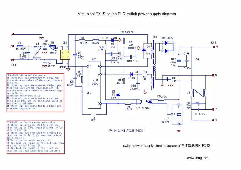
  1. Input Filtering and Protection: After entering the power board through the L and N terminals of the PLC, the industrial frequency 220V power first passes through a bidirectional low-pass filter network composed of C1, C2, C4, and L1. This design effectively filters out high-frequency interference and improves the purity of the power supply. Meanwhile, the bidirectional filters L1 and L2 further isolate high-frequency interference pulses from both inside and outside the power supply, ensuring stable system operation. F1 serves as an overload protection fast-acting fuse, while TH1 acts as a temperature fuse, together constituting a dual protection mechanism for the power supply.
  2. Rectification and Oscillation: The filtered AC power passes through F1 and TH1 into the full-wave rectification circuit, where it is rectified to obtain a direct current voltage of approximately 280V. This voltage is sent to the oscillation and voltage-stabilizing circuit centered on STRG6551. STRG6551 is a power oscillation module with an integrated switching tube. Its 4 and 3 pins are the power supply terminals, while 1 and 2 pins are internally connected to the source and drain of the power switching tube. Additionally, pin 2 provides negative feedback for the switching operating current. Pin 5 is the feedback voltage input terminal, used to regulate the stability of the output voltage.
  3. Voltage Stabilization and Protection: The voltage induced by the secondary winding of the switching transformer TB1 undergoes rectification and filtering before serving as the working power for the PLC. To maintain voltage stability, the system employs an output voltage sampling circuit composed of R9, IC2, PC1, and other components. When the voltage changes, this change is converted into a variation in the input current on the PC1 optocoupler device, which is then fed into pin 5 of STRG6551 through R4. The comparison amplification circuit inside STRG6551 adjusts the conduction/cutoff time of the switching tube, i.e., controls the duty cycle of the oscillation frequency, to achieve stable output voltage.

Furthermore, the system boasts a comprehensive protection mechanism. When an abnormal load causes a sharp increase in current, the voltage variation across the sampling resistor R2 is introduced into pin 5 of STRG6551, reducing the output voltage to decrease the load current. When the voltage or current anomaly reaches a certain threshold, STRG6551 disconnects the driving circuit of the switching tube, causing the circuit to oscillate and protecting the subsequent circuit from damage.

III. Maintenance Methods and Practices

Faced with potential faults in the Mitsubishi F1S switching power supply, reasonable troubleshooting steps and scientific maintenance methods are crucial for improving maintenance efficiency. Here are some common maintenance methods:

  1. Routine Inspection: First, check whether the F1 and TH1 fuses are blown. If they are blown and there are no abnormal short-circuit points in the switching tube and load circuit, replacing the fuses generally resolves the issue. If the power still does not oscillate after replacing the fuses, further investigation is needed.
  2. Identify Fault Circuits: Disconnect the PLC motherboard, use a voltage regulator to adjust the input voltage to below AC100V, and connect a dummy load (such as a 100Ω 5W resistor). Short-circuit pins 1 and 2 of the PC1 optocoupler to make the voltage feedback signal zero. Power on and observe the power output. If there is output but not at a stable voltage, the fault lies in the voltage-stabilizing circuit; if there is no output, the fault is in the oscillation circuit.