Posted on Leave a comment

ACS800 Variable Speed Drive (VSD) Debugging Steps

I. Basic Local Control Process for ACS800 VSD

Ensure that the air switch is closed and the contactor is energized.
Press the LOC/REM key to switch to local control mode.
Press the FAR key to enter the parameter setting interface. Use the double arrow keys to navigate to the 99 parameter group, then use the single arrow keys to select item 04. Press ENTER to confirm. Here, you can choose between DTC mode (suitable for most cases) or SCALA mode. After selecting, press ENTER to save or ACT to exit.
Press the ACT key to return to the main operation interface.
Press the REF key, use the up/down arrow keys to input the desired parameter value, and then press ENTER to confirm.
Press the start key to begin operating the VSD.
To replace the displayed actual signal, follow these steps:
a. Press the ACT key to enter signal display mode.
b. Select the row you want to change and press ENTER.
c. Use the arrow keys to browse and select a new signal (such as actual motor speed – SPEED, transmission output frequency – FREQ, etc.).
d. Press ENTER to confirm the change or ACT to exit.

II. Data Upload and Download Operations

To upload set motor parameters to the CDP-312 panel:

Verify that item 98.02 is set to FIELDBUS and item 98.07 is set to ABB DRIVES.
Switch to local control mode (LOC).
Press the FUNC key to access the function menu.
Use the arrow keys to navigate to the UPLOAD function and press ENTER to execute the upload.
If you need to move the control panel, ensure it is in remote control mode first.
To download data from the control panel to the drive unit:

Connect the control panel containing the uploaded data.
Ensure you are currently in local control mode.
Press the FUNC key to access the function menu.
Navigate to the DOWNLOAD function and press ENTER to execute the download.
III. Achieving PLC and VSD PROFIBUS-DP Communication

After confirming that the communication module is installed and the DP network cable is correctly connected, follow these steps to set the parameters:

In local mode, use FAR and the arrow keys to enter parameter settings.
Set 98.02 to FIELDBUS to activate the RPBA-01 communication module.
Set 98.07 to ABB DRIVES to determine the communication protocol.
Configure items 10.01, 10.02, and 10.03 as needed to define the external control source.
Set 16.01 to YES to allow operation.
Select the fault reset signal source for 16.04.
From 11.01 to 11.08, set the source of the control word and given value.
In items 22.01 to 22.03, define acceleration/deceleration time and stop function.
For the 51 group of parameters, configure according to the fieldbus adapter module’s settings.
Adjust the actual signal transmission content in the 92 group as needed.
IV. Additional Parameter Setting Reference (Not Currently Used)

This section provides guidance on setting speed limits, protection functions, and parameter locking for future reference.

Note: Before making any parameter changes, ensure you fully understand their impact and consult a professional if necessary.

Posted on Leave a comment

Adjusting the Power Rating of ABB VFDs: A Step-by-Step Guide

Adjusting the Power Rating of ABB VFDs: A Step-by-Step Guide

When it comes to flexibility in power rating adjustments, ABB’s ACS510/ACS550/ACS350/ACS355/ACH550 Variable Frequency Drives (VFDs) offer a seamless solution. Whether you need to upgrade from a 1.1KW to a 5.5KW VFD or make any other power adjustment, these drives provide the capability to adapt to your specific requirements. This is especially beneficial in scenarios where you have a limited number of VFD main boards, like the SMIO-01C, and need to utilize them across different power ranges. Below is a detailed guide on how to access and modify the power rating parameters of these VFDs.

Accessing and Modifying Parameters

  1. Open the Parameter Table:
    • Navigate to the deepest level of parameters, which may include numbers like 0102 or any other displayed values.
    • If you see 9905, for instance, hold the UP (arrow up), DOWN (arrow down), and RETURN (button next to LOC on the upper left) buttons simultaneously for 3 seconds.
    • You will observe a flash on the screen, and the top line should display “PARAMETERS+”.
  2. Expand Parameter Groups:
    • Exit and re-enter the parameter groups.
    • Notice that the number of parameter groups has increased from 99 to a maximum of 120.
    • Navigate to parameter group 105.

Modifying Power Capacity

Follow these precise steps to adjust the power capacity:

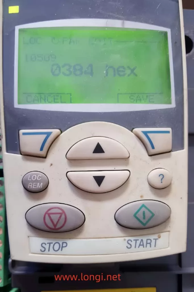
  1. Find and Modify Parameter 10509:
    • Change 105.09 to the desired current value.
    • Ensure the corresponding power value matches the VFD label. For example:
      • For ACS510-01-017A-4, change to 0174H.
      • For ACS510-01-031A-4, change to 0314H.
  2. Set 10502 to 1 and confirm.
  3. Set 10511 to 4012 and confirm.

Note: The order of these modifications is crucial. Any mistake may require you to restart the process.

Verifying Parameter Changes

  • Re-enter the parameter table.
  • Check if parameter 3304 (transmission capacity) reflects the correct modifications.

Important Considerations

  • The process outlined above modifies the power rating on the ABB drive motherboard (SMIO-01C). It does not alter the power of the drive board itself.
  • Despite the appearance of expanded power capabilities, the actual output power of the VFD remains unchanged unless the power board is also modified.
  • This guide is specific to ACS510/ACS550/ACS350/ACS355/ACH550 VFDs and is not applicable to the ACS800 series.

For assistance with power modification methods for ACS800 inverters, please reach out to us directly. Our team is here to help you navigate the intricacies of VFD power adjustments and ensure your equipment operates at its optimal capacity.

Posted on Leave a comment

Exploring the Circuitry and Modification Techniques of Frequency Inverter Transformers

In the realm of frequency inverter circuits, transformers have evolved significantly. While early models relied on traditional transformers wound with through-core inductor coils, modern, mature circuits predominantly feature integrated, sealed current transformers constructed using Hall elements and pre-current detection circuits. These are often referred to as electronic current transformers and are categorized as either standard or non-standard types.

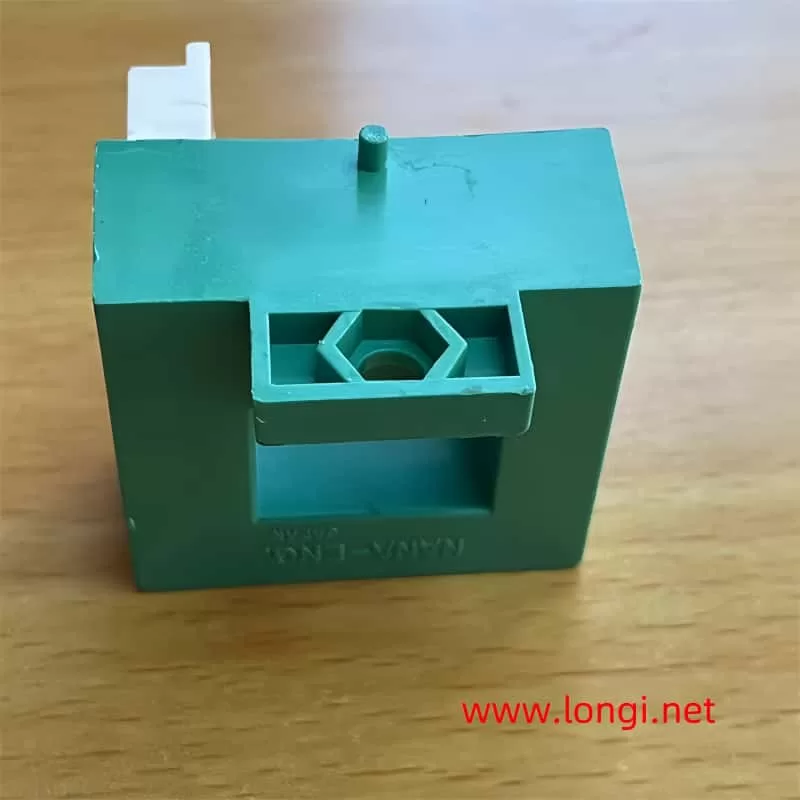
Physical picture of frequency converter current sensor

Standard electronic current transformers are readily available molded products in the market. For instance, a 10A/1V current transformer outputs a 1V signal for every 10A of current flowing through the circuit. On the other hand, non-standard types are custom-designed by frequency converter manufacturers and are not interchangeable. In case of damage, replacing them with the same model from the original manufacturer is usually necessary. However, with in-depth maintenance knowledge, different models can sometimes be used as temporary solutions until a permanent replacement is sourced.

The construction of electronic current transformers often involves the use of sealants, making them difficult to repair once damaged. This has led to much curiosity about their internal circuitry and repairability. During my experience repairing a Fuji frequency inverter, I needed to adjust the A/V ratio of the electronic current transformer, which required accessing its internal circuit. This prompted me to carefully dissect and map the internal circuits of current transformers from three different frequency inverter models, a process that was both challenging and rewarding.

At its core, an electronic current transformer is essentially a current-to-voltage converter circuit. The current transformer used in a Taian 7.5kW inverter serves as a representative example. The main body of the transformer is a circular hollow magnetic ring through which the U, V, and W output lines of the frequency inverter pass as the primary winding. As the output current of the frequency inverter varies, the magnetic field lines generated by the magnetic ring also change in density.

Embedded within the gap of this magnetic ring is a Hall element with four lead terminals. The Hall element, packaged in sheet form, has its packaging end face (also known as the magnetic field line collection area or magnetic induction surface) exposed to the magnetic field lines. The Hall element converts changes in magnetic field lines into induced voltage outputs.

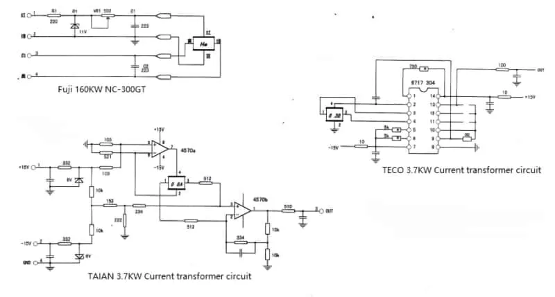
Internal circuit diagram of the current sensor in a frequency converter.

The circuit of the current transformer comprises the Hall element and a precision dual operational amplifier circuit, such as the 4570. For the Hall element to operate, a constant current of approximately 3-5mA must be supplied. In this circuit, the 4570A is configured as a constant current source to provide the necessary mA-level constant current for the Hall element (approximately 5.77mA in this case). This current is applied to pins 4 and 2 of the Hall element.

The induced voltage, which varies with the output current, is present at pins 1 and 3 of the Hall element and is applied to the input terminals 2 and 3 of the 4570B. The three pins are connected to a reference voltage (zero potential point), and any change in the input voltage at the two pins is amplified and output by the 4570B.

Electronic current transformers typically have four terminal components: two terminals supply power to the internal amplifiers (+15V and -15V), while the other two serve as signal output terminals (one grounded and one as the signal OUT terminal). In addition to powering the dual operational amplifier IC4570, the +15V and -15V are further stabilized to form a zero potential point that is introduced into the three pins of the 4570. When the frequency converter is off, the ground measurement at the OUT point should read 0V. During operation, it outputs an AC signal voltage proportional to the output current, typically below 4V.

If an electronic current transformer is damaged, it may output a higher positive or negative DC voltage in the static state (when the frequency inverter is off). This is often due to damage to the internal operational amplifier. When the frequency inverter performs a power-on self-test, it may display a fault code (sometimes not listed in the manual) and refuse to start or even operate with its parameters.

The current transformer circuit of a TECO 3.7kW frequency converter utilizes a programmable operational amplifier chip. Although I have not yet identified the specific model of this chip, modification tests have revealed some of its circuit characteristics. Experimental results indicate that pin 2 is the constant current power supply terminal, pins 3 and 4 are the input terminals of the differential amplifier, and pin 13 is the signal output terminal. By short-circuiting the solder gaps of pins 11, 12, and 13 in a stepwise manner, the amplification factor decreases; conversely, opening the circuit step-by-step increases the amplification factor. This adjustability allows for easier matching of the chip with frequency converters of different power outputs. I successfully applied this current transformer to a 45kW Fuji frequency inverter by taking appropriate measures.

It is important to note that the voltage and current detection signals of the frequency converter may be used by the program to control the output three-phase voltage and current. Therefore, when repairing or modifying the original circuit, it is crucial to maintain the original circuit parameters to ensure proper operation. Whenever possible, it is recommended to use original accessories to repair the frequency converter while preserving the original circuit form.

Posted on Leave a comment

Understanding and Repairing Brake Units in Frequency Converters

In the realm of industrial machinery, frequency converters play a crucial role in controlling motor speed and efficiency. However, when dealing with high inertia loads, such as in mining elevators or high-speed lifts, the motor can transition from an “electric” state to a “dynamic” state, temporarily becoming a generator. This phenomenon results in regenerative energy flowing back into the system, which can cause voltage spikes and potentially damage the frequency converter’s components. To mitigate these issues, brake units and braking resistors are often integrated into the system. This article delves into the workings of a brake unit, its circuit diagram, and troubleshooting tips.

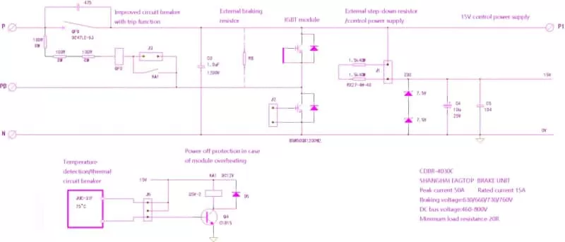
Structural diagram of braking unit

The Role of Brake Units

When a motor decelerates, brakes, or lowers a heavy load, the mechanical system’s potential energy can cause the motor’s actual speed to exceed the frequency converter’s set speed. This leads to a capacitive current in the motor windings, which generates excitation electromotive force, causing the motor to self-excite and generate electricity. This electrical energy is then fed back into the power grid. However, this regenerative energy can cause the voltage in the frequency converter’s DC circuit to rise sharply, potentially damaging the energy storage capacitors and inverter module.

To prevent this, brake units and braking resistors are used. A brake unit is essentially an electronic switch (IGBT module) that, when activated, connects the braking resistor to the DC circuit. This rapidly dissipates the motor’s regenerative energy as heat, keeping the DC circuit voltage within safe limits.

Circuit Analysis

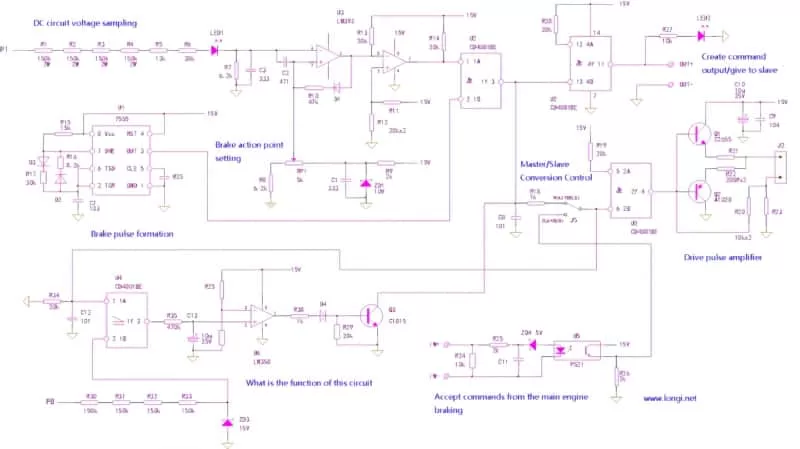
The brake unit’s control circuit typically includes a DC voltage detection circuit that triggers the electronic switch when the DC circuit voltage exceeds a certain threshold (e.g., 660V). Once the voltage drops below a lower threshold (e.g., 620V), the switch turns off.

In more advanced systems, the brake unit’s performance is optimized through pulse braking. Here, a voltage/frequency or voltage/pulse width conversion circuit controls the IGBT module’s on/off state. When the DC circuit voltage is high, the braking unit operates at a higher frequency or longer conduction cycle, and vice versa.

Electronic circuit diagram of brake unit control part

The CDBR-4030C Brake Unit

The CDBR-4030C brake unit, while not the most optimized in terms of structure and performance, is still effective in practice. It uses a dual-tube IGBT module, although only one tube is utilized, making it somewhat inefficient. The protective circuit combines electronic and mechanical trip circuits, with the QF0 air circuit breaker modified to trip when the module overheats.

Common Faults and Repairs

Faults in the brake unit often occur in the control power supply circuit, such as an open circuit in the step-down resistor or a breakdown in the voltage regulator. Additionally, moisture can reduce the insulation in the frequency converter’s DC circuit, leading to high voltage discharge and circuit board damage.

The brake unit’s control circuit typically includes an LM393 operational amplifier, a CD4081BE four-input AND gate, and a 7555 (NE555) timer circuit. Troubleshooting involves checking these components and their connections.

One unique feature of the circuit is the hysteresis voltage comparator, which prevents frequent output fluctuations by providing a certain hysteresis voltage. If the braking unit fails to operate correctly, it could be due to issues in this comparator or the voltage comparator connection.

Protective Measures

The circuit also includes protective measures to prevent damage to the IGBT module. For instance, if the module temperature rises to 75°C, a temperature relay triggers a trip, cutting off the brake unit’s power supply. Additionally, the circuit design ensures that if the braking resistor remains connected or the IGBT module fails, the system will shut down to prevent further damage.

Conclusion

Understanding the workings of a brake unit and its circuit diagram is essential for effective troubleshooting and repair. By analyzing the control principle and common faults, technicians can quickly diagnose and resolve issues, ensuring the smooth operation of frequency converters in industrial applications. With proper maintenance and repairs, brake units can provide reliable protection against voltage spikes and regenerative energy, prolonging the lifespan of frequency converters and their components.