Posted on Leave a comment

Based on the overall circuit of the VFD (Variable Frequency Drive), there are two malfunctions.

(A) Power Supply Fault Inspection:

Fault Status: After powering on, the entire device does not respond, and the operation display panel shows no display. The measured 24V and 10V control power at the control terminals are both 0V.

Fault Essence: The VFD’s switching power supply is not working.

Troubleshooting Approach: (1) Switching voltage fault; (2) Pre-charging circuit fault.

Troubleshooting Method:
(1) First check the power supply source of the switching power supply and whether the DC loop has a normal 530V voltage. If the DC loop voltage is 0V, it indicates a fault in the pre-charging circuit, such as an open charging resistor, damaged half-wave rectifier circuit, or poor contact of the normally closed contact of the contactor or relay. Repair the pre-charging circuit first and then check the fault of the switching power supply. Often, after repairing the pre-charging circuit, the VFD is also repaired. It is not necessary to focus too much on the switching power supply circuit at first.

(2) If the 530V, 265V, or 300V DC power supply for the switching power supply is available, do not focus too much on its voltage stabilization and oscillation circuit. First, check if there are any faults such as short circuits in the secondary load circuit of the switching transformer, such as a damaged cooling fan, an IC short circuit in the fault detection circuit, or a breakdown of the rectifier diode. The fault rate on the load side of the switching power supply is higher, while the problems in the oscillation and voltage stabilization links are less common.

The troubleshooting approach and order determine the efficiency of the repair work. From the perspective of the entire circuit, checking the pre-charging circuit is a very important step and should be the first consideration when troubleshooting the fault of a non-working switching power supply.

(B) Fault Inspection of the Inverter Pulse Circuit:

The section from the six PWM output terminals of the CPU to the intermediate buffer circuit is called the pre-stage circuit of the inverter pulse, while the drive circuit is referred to as the post-stage circuit of the inverter pulse, collectively known as the inverter pulse circuit.

Fault Conditions:

(1) Normal start-up operation, with normal output frequency indication on the operation display panel, but no three-phase output voltage.
(2) Normal start-up operation, with normal output frequency indication on the operation display panel, but unbalanced three-phase output voltage.
(3) OC fault occurs immediately after pressing the start button.
(4) OC fault occurs during operation.
(5) Light-load operation is normal, but motor with load jumps or encounters OC fault.

Essence of the Faults and Inspection Approach (Corresponding to the Five Fault Conditions):

(1) Several factors may contribute: a. Loss of +5V* power supply on the input side of the drive circuit’s optical coupler; b. Damage to the buffer of the pre-stage pulse circuit; c. Uncertainty of the CPU’s relevant control signals or damage to related control pins; d. Misoperation of the fault protection circuit, resulting in the locking of the pulse pre-stage circuit by the fault signal.

Special attention should be paid to the pre-stage circuit of the inverter pulse signal, such as tri-state triggers and buffer circuits, which may be directly controlled by voltage and current detection and protection circuits. When the protection circuit misoperates, it may clamp and block the transmission of six pulse signals. The concept of the fault protection circuit participating independently in pulse transmission control should be kept in mind. Although faults caused by a and b are more common, those caused by c and d often constitute difficult faults, and a lack of inspection approach in this regard may lead to detours in repair.

(2) Three factors may contribute: a. Damage to the opto-coupler of the drive circuit, preventing the normal transmission of inverter pulse signals; b. Increased internal resistance of the inverter module, leading to poor conduction in three upper-arm IGBT modules. Therefore, the three drive circuits may not be equipped with IGBT voltage drop detection circuits, resulting in a failure to report OC faults; c. Malfunction of the pre-stage pulse circuit or the CPU inverter pulse output pin, causing the inverter pulse to be missing in one or two channels.

Don’t focus solely on the post-stage drive circuit, as the inverter pulse of the pre-stage may not be input to the drive circuit. Especially, consider whether the module is faulty or the internal resistance of the inverter module has increased. Failing to consider factor c may also lead to difficult faults.

(3) Several factors may contribute: a. Defects in the post-stage drive circuit itself; b. Insufficient load capacity of the power supply of the drive circuit, such as loss of capacitance in filter capacitors and low efficiency of rectifying diodes (increased forward resistance and decreased reverse resistance); c. Defects in the inverter module.

Dynamic and static testing (voltage testing) of the drive circuit may appear normal, but it is necessary to test the current output capability of the drive circuit. Pay attention to factors b and c.

(4) Several factors may contribute: a. Load capacity of the drive circuit and internal resistance detection of the inverter module; b. Three-phase output current detection circuit; c. Reference voltage circuit in the fault detection circuit; d. User load-related reasons.

Pay attention to the influence of factors b, c, and d. Defects in the three-phase detection circuit itself or shifts in the operating point may cause false OC fault reports. Deviations in the reference voltage of the fault detection circuit may lead to inaccurate current detection and false OC fault reports. If all checks are fine, look for the cause on the production site, not excluding issues related to the load. Factors b and c may again fall into the category of difficult faults.

(5) Three factors may contribute: a. Insufficient current (power) output capability of the drive circuit; b. Defects in the inverter module, resulting in increased internal resistance; c. Issues with the load circuit, such as a faulty motor, not necessarily a fault of the VFD.

Abnormal operation of the VFD does not necessarily indicate a problem with the VFD itself. It is recommended that users try replacing the motor. Consider factors b and c, and sometimes factors outside the VFD.

Posted on Leave a comment

The repair process of an unlicensed VFD caught up with lightning speed

In movies and TV shows, when a Taoist from Maoshan encounters an urgent and difficult situation, he often recites a curse: “The Supreme Old Lord is as sick as a law… If something difficult happens, it should be solved by the curse.”. If there is an urgent VFD repair, we can also recite a few mantras and find the “smart” method for quick maintenance.
On a rainy day, thunder and lightning flash. The door of the maintenance department was suddenly forcefully pulled open by someone. Three or four strong men, carrying an unmarked 75kW VFD, strode in and asked, “Our workshop is for refining silver, and the frequency converter was damaged by lightning.”. Urgent use! Can the malfunction be detected and repaired within three hours. Okay, don’t bargain; If you don’t have diamond, don’t take on porcelain work. Let’s quickly change the door. It’s not just you who can fix VFD.
This VFD may be able to earn half a month’s salary. No second words, fight!

I roughly inquired about the damage to VFD. During operation, due to lightning strikes introduced from the three-phase power supply, even the main power switch in the workshop tripped. Close the power switch of VFD again, there is a popping sound, and the switch jumps open again.
In this situation, there must be a short circuit fault in the three-phase rectifier circuit of VFD. Instead of being busy with power on, use the resistance range of the multimeter’s R, S, T power input terminals and U, V, W output terminals to determine the resistance of the main circuit with the P and N terminals of the DC circuit. There is a short circuit phenomenon in the measurement, rectification, and inverter power circuits. Detailed inspection after disassembly revealed that two rectifier modules were damaged, one inverter module was broken, and the energy storage capacitor was tested and found to be fine.
The repairman asked, “Isn’t it enough to replace these three faulty parts?”? Answer: Don’t be impatient. Due to the introduction of lightning strikes within VFD, the situation is complex and the quality of the control circuit board is unclear. If the inverter power module is damaged, it will have an impact on the driving circuit. If there is a hidden fault, the replacement module will be damaged again. Further investigation is needed to determine whether to replace the module.
Key contents to be checked: 1. Whether the CPU motherboard is damaged, especially whether the CPU chip is damaged; 2. Inverter pulse transmission circuit, including driving circuit and inverter pulse front-end circuit. Especially for the driving circuit, the triggering terminal circuit of the IGBT should be checked for any open circuit or negative pressure power supply; 3. Other circuits, whether the control terminal circuit has been damaged by lightning strikes, and whether the control circuit (fault detection circuit, etc.) has been damaged.
The key among them is that as long as the CPU can output six inverter pulses, repairing other faults should be easy.

(A) Power on the switch power supply or troubleshoot the switch power supply:
Remove the CPU motherboard and power/driver board from the inverter casing and place them on the maintenance workbench. Power should be supplied to the switch power supply of the circuit board first, or the switch power supply should be repaired first to facilitate troubleshooting of other circuits. I tested the power supply terminals of the switching power supply and the filtering capacitor at both ends of the secondary rectification circuit of the switching transformer, and there was no short circuit phenomenon. It is possible to power on the switching power supply. The power supply source of the Shunxia switch power supply is directly taken from the 530V DC circuit of the DC circuit. If measured on the circuit, the drain (collector) of the switching transistor of the switching power supply should be connected to the P-terminal of the DC circuit, and the source (emitter) should be connected to the N-terminal of the DC circuit.
Alright, connect the 500V DC maintenance power supply to the power supply terminal of the switch mode power supply (pay attention to polarity, it can be bad if connected in the opposite direction), it’s not bad! The corresponding changes in characters during the startup period on the operation display panel indicate that the switch power supply and the peripheral circuit of the CPU chip are basically working normally, and the CPU is also good.
(B) Release the OH (module overheating) fault alarm:
After the startup character on the operation display panel flashes, an OH (module overheat) fault code is reported. Press the RST reset button on the operation display panel, OH disappears once, and it is displayed again, unable to reset. At this time, the frequency converter is in a fault locked state and refuses to accept operating signals, making it impossible to detect whether the inverter pulse transmission circuit is normal. The OH alarm must be disarmed. Observing the main circuit, two normally closed contact type thermal relays are installed near the heat sink module. When the circuit board is disconnected from the main circuit, it is equivalent to the temperature sensor’s normally closed point breaking, reporting an overheat signal. Find the corresponding temperature sensor terminals on the circuit board, short circuit them with wires or solder, and there should be no OH fault reported. Some frequency converters use thermistors to detect the temperature of the module. When the terminal is open, an OH fault will also be reported. Simply remove the temperature sensor and insert it into the corresponding terminal on the control board. Still report OH, don’t worry, there may be related temperature detection signals sent to the control board.
Observe the socket and lead of the cooling fan, which is a three wire fan. Two wires are the positive and negative terminals of the 24V power supply, and one wire is the signal wire. Return the operation/fault signal to the control board. If you remove the fan and plug it back into the control board, it would be too troublesome. There is a simple way to find the positive and negative wires, and test connecting the third wire to the positive and negative power supply terminals respectively. When this wire is connected to the positive power supply terminal, the OH fault code on the operation display panel disappears.
(C) Release Uu (undervoltage) and input phase loss alarm:
After a brief moment of joy, the operation display panel showed another Uu (undervoltage) fault, and the frequency converter was still in a fault locked state.
When the switching power supply adopts 265V (or 300V) DC power supply, we disconnect the control board from the main circuit and separately supply 265V (or 300V) DC power to the switching power supply. Most of the operation panels will report Uu faults (some frequency converters, DC circuit voltage detection signals are obtained in the secondary rectification circuit of the switching transformer, so Uu faults will not be reported), because the input of the DC circuit detection circuit is in an open circuit state, and the circuit output is an undervoltage signal. From the DC circuit voltage introduction terminals (P, N terminals), find the input resistance network of the DC circuit detection circuit, a large high resistance circuit, seven or eight phases in series, because the switching power supply is 300V DC power supply at this time, directly introduce it into the DC circuit voltage detection circuit, or report a Uu fault. Short circuit a few resistors in the input resistor network (if there are 8 resistors, 3 can be short circuited for testing) to adapt to the 300V voltage output range.
Introduce a DC voltage artificially into the DC detection circuit and modify the detection to meet the requirements of the voltage input range. Some frequency converters may not report Uu faults, but they may also report “charging contactor not engaged fault”, while others may still report Uu faults. Don’t worry, there may be related voltage detection signals sent to the control board.
The charging contactor cannot be removed and connected to the control board in the main circuit. The frequency converter often has a status detection circuit for the auxiliary contact of the charging contactor. Due to the disconnection between the control board and the main circuit, the CPU detects that the auxiliary contact of the charging contactor is always in an open circuit state after the control board is powered on, and will also report Uu or “charging contactor not engaged fault”. Find the lead terminals of the auxiliary contacts of the charging contactor from the main circuit, determine the corresponding socket terminals of the control board, short circuit or solder the lead terminals with wires, and tell the CPU that the charging contactor has been closed.
After short circuiting the lead terminals of the auxiliary contacts of the charging contactor, the operation display panel finally stopped tripping Uu fault.
(D) Release OC (module overcurrent or output short circuit) fault alarm:
After a brief moment of joy, the fault code no longer jumps. From the display on the operation display panel, it appears that the inverter has entered standby mode and can be started for maintenance of the inverter pulse transmission channel. Press the start/stop button on the operation display board, but the frequency converter does not respond. The user may have set it to terminal operation. Ask the repairman, and indeed. For the convenience of operation, if the control parameters can be modified (if there is a frequency converter manual at hand), or the operation can be changed to start/stop and frequency adjustment using the control panel; If it is inconvenient to modify the parameters, you can try inputting the operation and frequency signals from the control terminal. Measure the frequency and adjust the power supply to 10V for normal output. Short circuit it to the input end of the 0-10V frequency signal to input the highest operating frequency command for the frequency converter (it is not troublesome, but can also be adjusted with an external potentiometer). Short circuit the forward running terminal to the digital common terminal for a startup test, and the operation display panel will display an OC fault code. Of course, the frequency converter is still in a fault locked state and cannot accept the operation.
The power module cannot function without various comprehensive protections, but at this point, I really feel that these fault alarms are troublesome. However, if they are not resolved, the inverter pulse transmission circuit cannot be repaired. Slowly, when an alarm signal is issued, it will be tracked and released. Generally, when the control circuit board is disconnected from the main circuit, three or four faults will jump out. Pay attention to finding the source of each signal from each plug-in terminal, or from the input and output sides of the plug-in terminal or the optocoupler that transmits the signal, use wire short circuiting method to force the CPU to input a “normal” signal and release the fault lock state.
The OC signal is mostly sent back to the CPU by the IGBT voltage drop detection circuit (IGBT protection circuit) of the driving circuit. When there is a fault in the output current detection circuit, an OC fault will also be reported, but this situation is relatively rare. Following the principle of easy first and difficult later, the OC signal returned by the driving circuit can be released first, and then the output current detection circuit can be detected.
The commonly used ICs for driving circuits are PC923, PC929, and A316J. The former uses the OC signal output by the internal IGBT protection circuit of PC929, which is then sent to the CPU through an external optocoupler. Find the optocoupler connected in parallel with PC929, and short-circuit its input side with a soldering iron to release the OC alarm (it is a fast method, not a good method); The latter, the 5 pins of the driver chip A316J are the OC signal output pins, which are separated from the copper foil strip to isolate the transmission of OC signals; But this method is not very convenient. Although it blocks the transmission of OC signals, it is advisable to check whether the CPU and the front-end inverter pulse transmission circuit have output inverter pulse signals. However, the drive IC itself is still in a fault locked state, which is not conducive to repairing the drive circuit.
A good solution is to manually input an IGBT “normally open” signal to the IBGT detection circuit, so that the driving IC itself no longer reports OC faults during the input inverter pulse period. The general driving circuit is implemented by the lower three arm driving circuit to detect the voltage drop of the IGBT transistor. The trigger terminal is used to short circuit the output end of the inverter pulse to the OV end of the driving power supply (the connection point with the N end of the main circuit), which is also relatively easy to find.
(E) Perform maintenance on the drive circuit:
Finally, the frequency converter can accept the startup signal. Looking at the gradually increasing output frequency indicator displayed on the control panel, I breathed a sigh of relief, indicating that the CPU circuit and control terminal circuit are both good. The repair of the frequency converter is basically without any suspense.
Measure the six inverter pulse input terminals of the driving IC, and there is a significant voltage change in the start and stop states. The six inverter pulses from the CPU motherboard have been input into the driving circuit intact and undamaged. The CPU motherboard is good! Measure the output status of six inverter pulses from the pulse output terminals of the power/driver board, and check if the negative cutoff voltage is normal and if there are normal pulse outputs. Does the voltage amplitude and current amplitude of the pulse output meet the normal requirements? Due to the damage of the IGBT causing impact on the driving IC, there are two driving circuits that cannot output pulse signals normally. This is simple. A power amplifier consisting of a driver IC and a rear stage consisting of two transistors was found to have damaged components. After replacement, all six inverter pulses were output normally.
The maintenance process has been declared completed. The entire maintenance process took exactly 45 minutes. After the maintenance is completed, it seems like we won a small battle so happily. The next task is to replace and purchase modules.

Throughout the entire maintenance process, four strong men were eagerly staring at the frequency converter, including one electrician who was extremely excited: he had learned and really had real skills. I didn’t expect it to be so troublesome. Blowing up a module is not as simple as replacing it.
To the repairman, the control circuit has been repaired, but there is no power module at hand. Then, you can go to the same city to “search” for it. If not, it will only be sent from outside the city. You will have to find your own way to delay your silver refining.
The four repairmen all laughed and said, “No problem, no problem. Please hurry up and send the package.”.
The various methods used during the maintenance process are scattered in my other blog posts, but they belong to local maintenance methods. For actual maintenance, sometimes there is a small gap between what is explained by a single unit circuit, which is difficult to understand. Through the description of a specific maintenance example process in this article, the application of various maintenance methods can be integrated and integrated.

Posted on Leave a comment

Analog circuits used in VFD fault detection circuits

The main circuit of the fault detection circuit is still composed of an operational amplifier. Usually, the operational amplifier is connected to the following types of circuits, completing three tasks of signal analog amplification, comparative output, and precision rectification.
(A)、 Inverting amplifier circuit:

Operational amplifier reverse amplification circuit

An operational amplifier has excellent characteristics such as high input impedance (without using signal source current), low impedance (with good load characteristics), amplification of differential mode signals (the difference between two input signals), suppression of common mode signals (with the same polarity and size of the two input terminals), and the ability to provide linear amplification for both AC and DC signals.
The figures (1), (2), and (3) in the circuit form are inverting amplifiers, where the output signal is in opposite phase to the input signal, also known as inverting amplifiers. The circuit has a dual amplification effect of voltage and current on the input voltage signal, but in small signal circuits, only the amplification and processing of the voltage signal are emphasized. The voltage amplification factor of a circuit depends on the ratio of R2 (feedback resistance) to R1 (input resistance). R3 is the bias resistor, and its value is the parallel value of R1 and R2. Due to the different values (ratios) of R2 and R1, three types of signal transmission functions can be completed, namely, forming three signal processing circuits: inverter amplifier, inverter, and attenuator. (1) The circuit is an inverting amplifier circuit with an amplification factor of 5; (2) The circuit is a inverter, which plays a reverse phase output role on the input signal and has no amplification factor, so it cannot be called an amplifier. Or input a 0-5V signal, then output a 0-5V inverted phase signal; (3) The circuit is an attenuator circuit. If a 0-10V signal is input, the output is 0-3. A 3V inverted signal is a proportional attenuator.
Figures (1), (2), and (3) have two characteristics of the circuit: 1. The input and output signals are reversed; 2. Whether it is an amplification, attenuation, or inverting circuit, the output signal maintains a proportional output relationship with the input signal, which can be broadly referred to as an inverting amplifier because the amplification factor of the inverter is 1, and the attenuator precisely utilizes the amplification effect of the circuit.
It is interesting that these three types of inverting amplifiers have applications in current and voltage detection circuits. Taking the current detection circuit as an example: This is because the current transformer connected in series to the three-phase output terminal has an amplifier built-in, and the output signal has reached a voltage amplitude of volts, while the input signal amplitude of the CPU must be within a voltage amplitude of 5V or less. Therefore, some reverse current signal processing circuits use reverse amplifiers with a certain amplification factor; Some use inverter circuits, which only perform inverter processing on the signal based on the polarity requirements of the CPU input voltage signal, without the need for further amplification; Some circuits are adapted to the signal amplitude range of the later stage circuit, and even use attenuator circuits to attenuate the voltage signal from the current transformer before sending it to the later stage circuit.
The power supply of the analog signal circuit in the detection circuit is generally powered by both positive and negative 15V dual power sources according to the requirements of amplifying AC signals. Based on the circuit form of the inverter amplifier and the circuit characteristics of the operational amplifier, we can find the corresponding detection method:

  1. According to the characteristics of the inverting amplifier, when a positive signal voltage is input, the input voltage must be negative below 0V, and vice versa, the output voltage must be positive above 0V, with 0V (ground) as the reference potential. To determine whether it is in a normal state based on the static circuit values of the circuit and input/output pins;
  2. Identify whether the circuit in this stage is an amplifier, inverter, or attenuator. Based on the ratio of input resistance to feedback resistance, the output voltage value can be roughly calculated to determine whether the circuit is in a normal state;
  3. According to the characteristic that the circuit has an amplification (or attenuation) effect on differential mode signals and a zero amplification effect on common mode signals, when short circuiting two input terminals, the output voltage should be close to the zero potential value; Alternatively, if there is a positive voltage (or negative voltage output) at the output terminal, but two input terminals are short circuited, the output voltage immediately drops (or rises) to around 0V. The circuit is good and can transmit signals normally.
  4. If the input voltage value can be artificially changed, the output voltage will inevitably change accordingly, which can be used to determine whether the amplifier is in a normal state.
    [Fault Example 1]
    After a certain frequency converter is powered on, an OC fault is reported, and the fault reset is invalid. The current detection circuit, as shown in the diagram (1), has an output voltage of+12V. The CPU reports an OC signal after power on due to a serious overcurrent signal input. Short circuit the 2 and 3 pins of the operational amplifier with metal tweezers, measure that there is no change in the output circuit of pin 1, and it is still+12V. It is judged that the operational amplifier is damaged. After replacement, the fault is eliminated.
    [Fault Example 2]
    A certain frequency converter outputs an undervoltage signal after being powered on, and detects the electrogram (2) circuit. The input voltage is -3V, but the output voltage is 0. 7V, indicating a malfunction of the amplifier in this stage. A 10k resistor was connected in series with an external DC 12V power supply, and the output voltage did not change when input to the reverse input terminal. It was determined that the amplifier in this stage was damaged, and the fault was resolved after replacement.
    (B)、 In phase amplifier and voltage follower circuit:
In phase amplification circuit and voltage follower circuit

The circuit shown in Figure (1) is a typical circuit form of a in-phase amplifier, which is also one type of amplifier circuit. The input signal enters the same phase end of the amplifier, and the output signal is in the same phase as the input signal. The voltage amplification factor of the circuit is 1+R2/R1. It is also used for amplifying analog signals in fault signal detection circuits. When R2 is short circuited or R3 is open circuited, the output signal has the same phase and equal magnitude as the input signal, so (1) the circuit can further evolve into (2) and (3) circuits.
The above figures (2) and (3) show the voltage follower circuit. The output voltage completely tracks the amplitude and phase of the input circuit, so the voltage amplification factor is 1. Although there is no voltage amplification effect, it has a certain current output ability. The circuit plays a role in impedance transformation, improving the load capacity of the circuit and reducing the mutual influence of high impedance in the signal input circuit and low impedance in the output circuit. When used as a circuit follower, sometimes a single power supply is also used.
(1) The circuits (2) and (3) are also used in fault detection circuits for amplifying analog signals and processing reference voltage signals.
Based on the characteristics and functions of the circuit, the detection method can be obtained as follows:

  1. (1) The circuit is a in-phase amplifier circuit, and the output voltage amplitude and polarity are proportional to the input voltage. The voltage amplification factor of this stage is about 6 times. When the input voltage value is 1V, the output voltage is approximately 6V. It is possible to determine whether the circuit is in a normal state based on the calculation of input and output voltage values;
  2. (2) (3) The circuits are all voltage follower circuits, and the output voltage is completely tracked by the input voltage. The output voltage should be equal to the input voltage, which can be used to determine whether the circuit is in a normal state.
  3. By short circuiting two input terminals or manually changing the input voltage, the corresponding changes in the output voltage can be measured to determine whether the circuit is in a normal state.
    [Fault Example 1]
    A certain frequency converter experienced an OH fault when powered on. The reference voltage circuit of the temperature detection circuit, as shown in Figure (2), has an output voltage of 1V. This machine is a voltage comparator circuit, and its input voltage is measured to be 5V. Under normal conditions, the output voltage should also be 5V. After cutting off the output load circuit, the output voltage remains at 1. 2V, it was determined that the amplifier in this stage was damaged, and the fault was resolved after replacement.
    (C) Precision positive and negative half wave rectifier and full wave rectifier circuits:
Precision half wave and full wave rectifier circuits

The AC voltage signal from the current transformer needs to be rectified into DC voltage through subsequent half wave or full wave rectification circuits, and then sent to the CPU for current display and control. Precision half wave or full wave rectification circuits are also used for processing and amplifying analog signals. Ordinary rectification circuits use diodes as rectification devices, but diode rectification has drawbacks such as nonlinear distortion and dead zone voltage. Especially when used for small signal rectification, it will cause output signal distortion and output errors. By utilizing the amplification effect and deep negative feedback effect of the operational amplifier, a diode is added to the amplification circuit. By utilizing the unidirectional conductivity characteristics of the diode, different depths of negative feedback are introduced to the input positive and negative half wave signals. The input μ V level signal can be rectified in a dense manner, and the circuit itself also has a voltage following or amplification effect.
The above figure (2) shows a precision negative half wave rectification circuit. The circuit will perform precision rectification on the input negative half wave signal and output it in reverse phase. For the positive half wave input signal, the connection of D1 introduces deep negative feedback to the amplifier; At the beginning of the negative half wave input signal, due to the signal input amplitude being smaller than D1 and D2, both are in the cut-off state, and the circuit is in an open-loop amplification state. A small signal input will cause the output pin voltage to be greater than -0. 7V, D1 conduction, D2 reverse bias cutoff; The series connection of D2 and R125 introduces moderate negative feedback (the resistance of R125 can determine whether the current circuit is a rectifier or a rectifier amplifier, and the current circuit is a precision rectifier with no amplification effect), which is equivalent to an inverter amplifier, and the output is inversely correlated with the input signal.
The difference between the circuit in Figure (1) and Figure (2) is that the polarity of the two diodes in the circuit is opposite, making it a precise rectification circuit for the input positive half wave signal. The principle of rectification is the same.
By adding a half wave rectifier circuit and an inverse summation circuit, as shown in Figure (3), the positive and negative half waves are input and output in reverse to obtain a full wave output voltage waveform, forming a high-precision full wave rectifier circuit.
In fault detection circuits, rectifier circuits are often used to sample the three-phase output current signal, which is rectified and amplified as an analog voltage signal (current detection signal) input into the subsequent fault signal processing circuit and CPU circuit, used for overload alarm and sampling processing of operating current.
The input of the circuit is an AC voltage signal, while the output is a DC voltage signal. Most circuits are rectifiers, and some circuits are rectifier amplifiers.
Detection method:

  1. Rectifier circuit: The input side is AC voltage, and the output side is DC voltage. The two measured values are relatively close.
  2. Rectifier amplifier, with AC voltage on the input side and DC voltage on the output side. The output DC voltage value is higher than the input AC voltage value.
  3. By short circuiting two input terminals or manually changing the input voltage, the corresponding changes in the output voltage can be measured to determine whether the circuit is in a normal state.
    [Fault Example 1]
    A certain frequency converter experienced an OC fault when powered on. The output voltage of the current detection circuit as shown in Figure (2) was 13V. After unplugging the lead terminal of the current transformer, the amplifier in that stage still had 13V. It was determined that the rectifier circuit was damaged and the fault was resolved after replacement.
    (C) Circuit for voltage comparator, step voltage comparator, and window voltage comparator:
    The above-mentioned circuits are all used for amplifying and rectifying analog signals, and their output signals still have analog signals, which can be called analog signal (amplification) processing circuits. However, in the following voltage comparison and other circuits, the output is a switch signal. The circuit has left the scope of analog amplification and seems to have entered the field of “digital circuits”, using analog circuits as digital circuits for application.
Three types of voltage comparator circuits

The function of a voltage comparator is to compare the magnitude of two input voltage signals. In Figure (1) of the circuit, the voltage at the same phase input end of the amplifier is the voltage divider value 2 of R2 and R3 resistors to+5V. 5V, known as the reference voltage value, compares the input signal with this reference value. When it is higher than this value, it outputs a 0V low-level signal. When it is lower than the low value, it outputs a+15V high-level signal. Circuit, also known as a single value comparator, the output state of the circuit depends on a value (a point) of the input signal voltage -2. 5V.
If the two-stage voltage comparator is connected to the circuit shown in Figure (2), it becomes a stepped voltage comparator. The circuit has one input signal and two output signals. The N1 and N2 voltage comparators input the same signal voltage, but the reference voltage values at the same phase input terminals of the two-stage circuit are different. The N1 reference voltage is 6. The reference voltage value for 6V and N2 is 3. 3V. When the input signal gradually increases from 0V to 3. When the voltage is above 3V, the output state of N2 first changes to low level; N2 has an input signal value greater than 6. At 6V, there is only a low-level signal output. When the circuit in Figure (2) is used for voltage detection in the DC circuit, when the regenerative energy generated by the load motor is fed back to the DC circuit, causing the DC circuit voltage to rise to a certain value, N2 first outputs a braking action signal, connects the braking resistor to the DC circuit, and consumes the voltage increment; If the voltage continues to rise, N1 will output an OU overvoltage signal, and the frequency converter will shut down for protection.
If the two-stage voltage comparator is connected to the circuit shown in Figure (3), it constitutes a window voltage comparator circuit. Compared to single-stage voltage comparator circuits, window voltage comparators can be referred to as dual value comparators. The circuit has two benchmark comparison values and outputs one signal. When the input signal is ≥ reference voltage 1 ≤ reference voltage 2, the circuit output state transitions. Within a range of the intermediate value of the input signal, the output state remains unchanged. The circuit in Figure (3) is a ground fault signal processing circuit. The in-phase end of the N1 amplifier is the voltage divider of R46 and R50 to+15V, while the reverse end of the N2 amplifier is the voltage divider of R81 and R69 to -15V. The input three-phase current sampling signal enters the reverse input terminal of N1 and the in-phase input terminal of N2, and is compared with the positive and negative partial voltage values, respectively. Whether it is the positive half wave or negative half wave of the input signal, as long as it is greater than the two reference values, a ground short circuit signal will be reported.
The voltage comparator uses digital circuits, which can flexibly set the reference voltage based on the signal amplitude, making it more convenient than using digital circuits. In addition, the circuit in Figure (3) adopts an operational amplifier circuit with an open collector output, which can achieve parallel output at the output end, making the circuit more concise. If a regular amplifier is used, the output signal also needs to be isolated by two diodes and connected together in parallel.
Three types of voltage comparator circuits are commonly used to convert analog signals of detected current or voltage into switch signal – fault signal output, for implementing control actions and shutdown protection.
Detection method:

  1. The amplifier output has only two level states, low level, close to the ground level of the power supply or negative power supply value; High level, close to positive power supply value;
  2. If the voltage value of the inverting input terminal is lower than that of the in-phase input terminal, the output is low level; otherwise, the output is high level.
  3. By short circuiting two input terminals or manually changing the input voltage, the corresponding changes in the high and low levels of the output terminals can be measured to determine whether the circuit is in a normal state.
    (E) Hysteresis comparator circuit:
    It is also one of the voltage comparator circuits. The circuit in Figure (3) of the voltage comparator, also known as the hysteresis voltage comparator circuit. The voltage comparator circuit can be upgraded to a hysteresis comparator circuit by introducing an additional positive feedback circuit. Hysteresis comparator circuits are referred to as voltage comparator circuits with hysteresis characteristics. If ordinary voltage comparison is regarded as “voltage point comparison”, hysteresis comparator can be regarded as a comparator circuit for “voltage range comparison”. Usually, we hope that the output state of the circuit is stable enough, and comparing the voltage at a “point” can cause instability in the output state due to frequent output. Improving the “point” comparison of the input circuit to “segment” comparison can effectively solve this problem – within a “segment value” of input voltage variation, the output state remains unchanged. Figure (2) shows a positive feedback branch composed of R4 and D1, which converts the “point” comparison characteristic of the circuit into a “segment” comparison characteristic.

The control principle is briefly described as follows:
Assuming that the circuit in Figure (2) is used for processing the braking action signal, the input signal is the voltage sampling signal of the DC circuit. When the voltage of the DC circuit rises abnormally due to the energy feedback from the load motor, reaching 680V, the input voltage value of Vin reaches 9. When the voltage is above 5V and higher than the reference voltage at the reverse end of the amplifier, the amplifier outputs a low-level signal, and the subsequent braking circuit acts, connecting the braking resistor to the DC circuit to consume the voltage increment; Due to the consumption effect of the braking resistor, the input voltage value of Vin quickly drops to 9. Below 5V, but the braking signal is still being output, and it does not mean that the DC circuit voltage slightly drops, causing the braking signal to disappear. This indicates the role of the hysteresis comparator. The braking circuit continues to operate until the DC circuit voltage returns to below 620V, and the sampled input voltage is below 7. The braking circuit only stops working at 5V.
When the circuit is static, the voltage at the same phase end of the amplifier (7.5V) is higher than the voltage at the opposite phase end, and the output voltage is a high-level voltage of nearly 15V. R4 and D1 are introduced into the same phase end circuit, artificially raising the same phase end voltage to 9. 5V. When the input voltage is above 9. At 5V, the circuit output state reverses and the output end becomes low level. D1 reverse bias cutoff, feedback loop interruption, and reference voltage at the same phase end restored to 7. 5 V partial voltage value. In this way, when the input sampling voltage is below 7. At 5 V, the brake signal stops outputting.
Hysteresis comparator circuits are commonly used for voltage detection in DC circuits, outputting braking signals and overvoltage/undervoltage fault signals.
The detection method is the same as the voltage comparator, omitted.

Posted on Leave a comment

How to conduct load testing on VFD drive circuits to solve the problem of normal no-load and load failure?

The voltage amplitude of the six driving pulses outputted by the driving circuit meets the requirements. For example, measuring the amplitude of the positive excitation pulse voltage in the AC range is about 14V, and the amplitude of the negative cutoff voltage is about 7.5V (different models may vary). After the above inspection of the driving circuit, most maintenance personnel believe that the machine can be installed, but an extremely important inspection step – the inspection of the current (power) output ability of the driving circuit! Many VFDs that we believe have been repaired normally will still expose more hidden faults during operation, leading to a certain repair rate.

VFD operates normally under no-load or light load, but after carrying a certain load, it may experience motor vibration, output voltage phase deviation, frequency jump OC faults, etc.
Cause of malfunction: A. Insufficient output capacity of the power supply current (power) of the driving circuit; B、 The driving IC or the post amplifier of the driving IC is inefficient, and the output internal resistance increases, resulting in insufficient voltage or current amplitude of the driving pulse; C. IGBT is inefficient, with increased internal resistance and increased pressure drop in the conduction tube.

The proportion of failures caused by reason C is not high, and is limited by the conditions of the maintenance department, such as the inability to provide rated load testing for the frequency converter. But for the hidden faults caused by reasons A and B, we can use the method of increasing the load on the driver to expose them and then repair them, which can reduce the repair rate to the lowest level.
The normal opening of IGBT requires not only sufficient excitation circuit amplitude, such as+12V or above, but also sufficient driving current to ensure its reliable opening, or to ensure its conduction under a certain low internal resistance. The essence of the causes of faults A and B mentioned above is that due to the insufficient power output capability of the driving circuit, although the IGBT can be turned on, it cannot be in a good low conductivity internal resistance state, resulting in output phase deviation, severe motor vibration, and frequency jump OC faults.

Let’s conduct a more in-depth analysis of the control characteristics of IGBT and identify the root cause of the fault.

I. Control characteristics of IGBT:
The common perception is that IGBT devices are voltage-controlled devices, which require a certain level of excitation voltage for gate bias control, without the need to draw excitation current. In low-power circuits, only digital gate circuits can drive MOS-type insulated gate field effect transistors. As an IGBT, the input circuit happens to have the characteristics of a MOS-type insulated gate field effect transistor, and can therefore also be considered a voltage-controlled device. This perception is actually biased. Due to structural and process reasons, a junction capacitance called Cge is formed between the gate and emitter junctions of the IGBT tube, which controls the turn-on and turn-off of the IGBT tube. In fact, the charging and discharging control of Cge is responsible for the control of the turn-on and turn-off of the IGBT tube. The +15V excitation pulse voltage provides a charging current path for Cge, which turns on the IGBT; the -7.5V negative pulse voltage “forcibly pulls out the charged charge” on Cge, which plays a role in rapidly neutralizing the charged charge, and turns off the IGBT.
Assuming that the IGBT tube only controls the on-off switching of a DC circuit with a zero operating frequency, and after the Cge is fully charged at one time, there is almost no need for charging and discharging control, it is reasonable to describe the IGBT tube in this circuit as a voltage control device. However, the problem is that the IGBT tube in the output circuit of the frequency converter operates at a frequency of several kHz, and its gate bias voltage is also a pulse voltage with a frequency of several kHz! On the one hand, for such high-frequency signals, the capacitive impedance exhibited by Cge is relatively small, resulting in a large charging and discharging current. On the other hand, to make the IGBT turn on reliably and quickly (striving to make the tube have a small internal resistance), it is necessary to provide as large a driving current (charging current) as possible within the allowable operating range of the IGBT. For the control of turn-off, it is also the same. It is necessary to provide a low-resistance (ohmic) external discharge circuit to discharge the charge on the gate-emitter junction capacitor very quickly!
As we all know, capacitors are energy storage components that do not consume power themselves, and are called capacitive loads. However, just like the principle of power transmission and distribution lines, in addition to the power supply having to provide reactive current (reactive power) for capacitive components, which increases the power capacity of the power supply, the reactive current inevitably brings losses in line resistance (line loss)! The power loss of the drive circuit mainly concentrates on the gate resistance and the conduction internal resistance of the final amplifier tube. We often see that the output stage of the drive circuit, especially for high-power VFDs, is actually a power amplifier circuit, often consisting of medium-power or even high-power transistors, several watts of gate resistance, and other components, indicating that the drive circuit of IGBT consumes a certain amount of power and needs to output a certain current.
From the above analysis, it can be seen that the IGBT tube used in the VFD output circuit should be a current or power drive device, rather than a pure voltage control device

II. The last testing content before installation:
To minimize the rate of rework, after conducting comprehensive testing on the drive circuit in sections 3 and 4, do not miss the inspection of the drive circuit’s load-bearing capacity.
The method is as follows:

Measurement circuit for driving circuit with load capacity

The above diagram shows the driving circuit of the U-phase upper arm of DVP-1 22kW Delta VFD. The GU and EU in the figure are pulse signal output terminals, which are externally connected to the G and E poles of the IGBT. When repairing the drive board, it has been disconnected from the main circuit. The dashed box represents the external measurement circuit. After powering on the power supply/driver board, in conjunction with start and stop operations, a DC 250mA current range is connected in series at points m and n, and an external measuring resistor of 15 Ω 3W forms a circuit to detect the current output capability of each drive circuit. The starting state is measured, and five output current values are all around 150mA, with one output current only 40mA. The reason for the OC trip after installation and operation is precisely because the driving capability of this drive circuit is greatly insufficient! In the shutdown state, the measured current output capacity of each negative voltage power supply is about 50mA, and the negative voltage power supply capacity is normal.
Connecting RC in series plays a current limiting role, and the principle of its value is to select resistance and power values that are equal to the gate resistance (the parameter value of DR45 in the above figure) to make the detection effect obvious.
After testing the power output capability of the driving circuit, it can be determined that the driving circuit is completely normal. During the testing process of connecting the drive circuit to the main circuit, please first use a low-voltage 24V DC power supply to power the inverter circuit. After testing the drive circuit and inverter circuit to be normal, restore the normal power supply to the inverter circuit. If there is no low-voltage DC power supply at hand, at least two 45W light bulbs or 2A fuse tubes should be connected in series in the inverter power supply circuit. After the machine is tested normally, the original power supply of the inverter circuit should be connected!
The above power on detection of the driving circuit is carried out after disconnecting from the main circuit (IGBT). When the whole machine is connected, the input and input sides of the driving circuit must not be measured. Interference signals may be introduced due to human body induction and meter probes, causing IGBT to be triggered and conduct incorrectly, resulting in module explosion!

The insufficient output capability of the driving circuit is caused by two reasons:
A、 The power supply capacity is insufficient. Under no-load conditions, when we detect the output positive and negative voltages, they often reach the normal amplitude requirements. Even under load (such as after connecting to IGBT), although the instantaneous charging capacity of Cge is insufficient, due to the short charging time, we often cannot measure the low voltage drop of the power supply. Without resistive loads, this hidden fault can hardly be detected! The common fault in the circuit is the loss of capacitance of the filtering capacitor, as shown in DC41 in the figure above. Due to the drying up of the electrolyte inside the electrolytic capacitor during long-term operation, its capacity has decreased from a few hundred microfarads to several tens of microfarads, and even to a few microfarads. In addition, there may be inefficient rectifier tubes, such as an increase in forward resistance, which can also cause insufficient power output capacity;
B、 The internal output circuit of the driving IC is poor, or the internal resistance of the rear amplifiers DQ4 and DQ10 increases due to conduction. If there is no low drop in the power supply voltage after load testing, and the output voltage of T250 is detected to be low, it is a T250 defect. Otherwise, replace components such as DQ4 and DQ10. The phenomenon of increased resistance values such as DR40 and DR45 is relatively rare.
It should be noted that the insufficient positive excitation voltage only manifests as severe motor vibration, output voltage phase deviation, frequent OC faults, and other phenomena. Although it may cause overcurrent in the DC component of the motor winding, it poses a danger to the module structure that cannot be put into operation and the signal will burst. The loss of the negative cutoff voltage (caused by a fault in the negative pressure power supply circuit, which blocks the negative gate bias circuit) indicates that it is normal when powered on. When the start button is pressed, the IGBT inverter module will emit a “pop” sound and immediately burst into failure! Why is this?

III. Hazards of IGBT cut-off negative pressure circuit open circuit:
Except for the damage caused by sudden short circuit of the load during full speed operation, the harm of all faults such as overcurrent, overload, and undervoltage is far less than the harm of open circuit of gate bias circuit to IGBT. Speaking of this, maintenance personnel will deeply understand that they should not suffer too much from such losses.
During the maintenance process, the gate resistor DR45 was missed, and during the installation process, only the trigger plug of the upper arm IBGT1 was carelessly inserted, forgetting to connect the lower arm IGBT trigger terminal, resulting in the IGBT2 drive signal introduction terminal being vacant. After power on, the start signal is not activated, and there is no problem. Once the start signal is activated, there is no discussion, and the module is damaged. In my long-term maintenance work, I have developed a habit of stopping for a while before starting the operation after powering on, and observing whether the drive pulse output terminal is properly connected. After checking that each connection is intact, press the start button again. I often feel that this slight point is of great importance – the driving circuit and inverter output circuit are both in a normal state, and only one signal terminal of the driving pulse is missing, which will inevitably cause serious damage to the IGBT module and driving circuit again, resulting in all previous efforts being wasted!

Equivalent diagram of IGBT junction capacitance

Just like bipolar devices – transistors, three wire components inevitably form three equivalent capacitors inside, while the Cge inside IGBTs is not parasitic, but formed by process and structure. Let’s not bother with Cce capacitors. The two capacitors, Ccg and Cge, can have a destructive effect on IGBT.
The above diagram shows the situation when the triggering terminal of the lower arm IGBT is open circuit. After power on, IGBT1 can maintain a reliable cut-off state by applying a negative cut-off voltage to the G and E poles due to the connection of the driving circuit. The reckless input of the frequency converter operation signal causes IGBT1 to be driven by a forward excitation pulse voltage and turn on. The C pole of IGBT2, the U terminal, immediately jumps to a DC high voltage of+530V. This jump voltage provides a charging return circuit for the Ccg and Cge capacitors. During the turning on period of IGBT1, IGBT2 is also driven by this charging current, and it is almost simultaneously turned on. The common connection of the two tubes forms a short circuit to the+530V power supply at the P and N terminals. With a loud bang, both tubes explode! If the signal terminal of the upper tube is empty and the lower tube is connected to the driving circuit, the conduction of the lower tube will also cause damage to both tubes for the same reason.
Assuming that there is a gate bypass resistor connected in parallel on the G and E poles of IGBT2 (such as the R side in the IGBT1 gate control circuit), it will form a bypass effect on the charging current mentioned above, and the possibility of the two transistors sharing the same circuit will be reduced. Assuming that during the conduction period of the upper tube, there is a cut-off negative pressure of about 7V between the G and E terminals of the lower tube, and the positive charging current is neutralized and absorbed by the gate negative bias, which is far from reaching the amplitude required to turn on the IGBT, then IGBT2 is safe. This is also why negative pressure is added to the control circuit of IGBT.
For frequency converters using IPM intelligent inverter modules, the driving power supply is often a single power supply without providing negative pressure. Is that the case?
From a design perspective, the shorter the lead of the IGBT drive signal, the better, in order to reduce the inductance effect of the lead; There should be a small resistance circuit between the E and E poles of the IGBT to fully bypass the interference signal current. The IPM module, driver circuit, and inverter main circuit are integrated inside the module, and the wiring between the driver circuit and IGBT is extremely short. According to data, even the gate resistance is omitted to reduce the wiring impedance. In the off state, IGBT ensures that the gate is in a low impedance grounded state, effectively preventing misleading conduction caused by interference signals, thus eliminating the need for negative power supply.

Posted on Leave a comment

Maintenance ideas and methods for VFD switching power supply

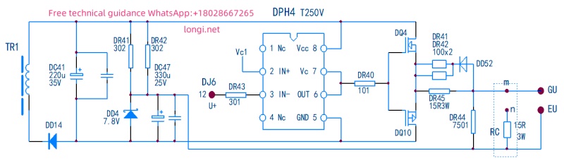
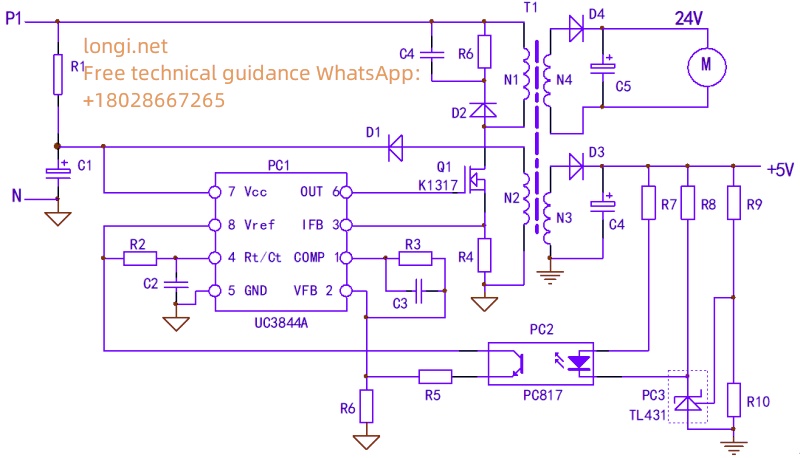
The switching power supply circuit of VFD can be completely simplified into the circuit model shown in the diagram, and the key elements in the circuit are included. And any complex switching power supply, after removing the branches, will still have a backbone like the one shown in the picture. In fact, in maintenance, it is necessary to have the ability to simplify complex circuits, and to identify these main threads in the seemingly disorderly extension of circuits. To learn from the skilled chef of Jieniu, train yourself that there is no overall switch power circuit in front of your eyes, only the direction of the various parts and veins – oscillation circuit, voltage stabilization circuit, protection circuit, and load circuit, etc.

Take a look at how many veins there are in the circuit.

  1. 1.Oscillation circuit: The leakage source and R4 of the main windings N1 and Q1 of the switching transformer are the paths for the working current of the power supply; R1 provides starting current; The self powered windings N2, D1, and C1 form the power supply voltage for the oscillating chip. The normal operation of these three links is a prerequisite for the power supply to oscillate.

Of course, the 4-pin external timing components R2, C2, and PC1 chip itself of PC1 also constitute a part of the oscillation circuit.

  1. 2,.Voltage stabilizing circuit: The+5V power supply of N3, D3, C4, etc., and components such as R7-R10, PC3, R5, R6 constitute the voltage stabilizing control circuit.

Of course, the PC1 chip and peripheral components R3 and C3 on pins 1 and 2 are also part of the voltage stabilization circuit.

3.Protection circuit: The PC1 chip itself and the 3-pin peripheral component R4 form an overcurrent protection circuit; The parallel D2, R6, and C4 components on the N1 winding form the protection circuit of the IGBT; In essence, the voltage feedback signal of the voltage stabilizing circuit, the voltage stabilizing signal, can also be regarded as a voltage protection signal. However, the content of protecting the circuit is not limited to the protection circuit itself. The initiation and control of the protection circuit are often caused by abnormalities in the load circuit.

  1. 4.Load circuit: N3 and N4 secondary windings and subsequent circuits are all load circuits. The abnormality of the load circuit will involve the protection circuit and the voltage stabilizing circuit, causing the two circuits to make corresponding protection and adjustment actions.

The oscillation chip itself participates in and constitutes the first three circuits. If the chip is damaged, all three circuits will strike together. The maintenance of three or four circuits is carried out under the premise that the chip itself is normal. In addition, like playing chess, we should use a global perspective and systematic approach to diagnose faults, and see the essence through phenomena. If there is a stop vibration fault, it may not be caused by damage to the oscillation circuit components. It may be a voltage stabilization circuit fault or an abnormal load circuit, which causes the internal protection circuit of the chip to start controlling and stops the output of PWM pulses. It is not possible to completely isolate each circuit for maintenance, and the appearance of a faulty component may exhibit the effect of “pulling one engine and moving the whole body”.

The oscillation chip itself participates in and constitutes the first three circuits. If the chip is damaged, all three circuits will strike together. The maintenance of three or four circuits is carried out under the premise that the chip itself is normal. In addition, like playing chess, we should use a global perspective and systematic approach to diagnose faults, and see the essence through phenomena. If there is a stop vibration fault, it may not be caused by damage to the oscillation circuit components. It may be a voltage stabilization circuit fault or an abnormal load circuit, which causes the internal protection circuit of the chip to start controlling and stops the output of PWM pulses. It is not possible to completely isolate each circuit for maintenance, and the appearance of a faulty component may exhibit the effect of “pulling one engine and moving the whole body”.

Switching power supply circuits often exhibit the following three typical fault phenomena (combined with Figures 3 and 9):
A、 The secondary load supply voltage is 0V. After the frequency converter is powered on, there is no response, and there is no indication on the operation display panel. The measured voltage of 24V and 10V at the control terminal is 0V. If the charging resistance or pre charging circuit of the main circuit is intact, it can be determined that there is a switch power supply fault. The maintenance steps are as follows:

1.First, use the resistance measurement method to measure whether there is any breakdown or short circuit phenomenon in switch Q1, and whether there is an open circuit in the current sampling resistor R4. The easily damaged component of the circuit is the switch tube. When it is damaged, R4 will increase in resistance or open circuit due to impact. The G-pole series resistor and oscillation chip PC1 in Q1 are often damaged by strong electrical shocks and need to be replaced simultaneously; Check for short circuits in the load circuit and eliminate them.

2.If the damaged parts are replaced or there are short circuited components that have not been detected, a power on inspection can be conducted to further determine whether the fault is in the oscillation circuit or the voltage stabilizing circuit.

Inspection method:
a、 First, check if there is an open circuit in the starting resistor R1. After normal operation, use an 18V DC power supply to directly power on pins 7 and 5 of UC3844 to separately power on the oscillation circuit. Measure that pin 8 should have a 5V voltage output; The 6 pins should have a voltage output of about 1V. The oscillation circuit is basically normal, and the fault is in the voltage stabilizing circuit;
If the voltage output of pin 8 is 5V, but the voltage of pin 6 is 0V, check the external R and C timing components of pins 8 and 4, and the peripheral circuit of pin 6;
If the voltage measured on pins 8 and 6 is 0V, the UC3844 oscillation chip is broken and needs to be replaced.

b、 Power on UC3844 separately and short circuit the input side of PC2. If the circuit vibrates, it indicates that the fault is in the peripheral circuit of the input side of PC2; The circuit still does not vibrate, check the PC2 output side circuit.

B、 Intermittent oscillation occurs in the switching power supply, where a “hiccup” or “squeaking” sound can be heard, or a “hiccup” sound cannot be heard, but when the display panel is operated, it lights up and turns off. This is a typical fault characteristic caused by abnormal load circuit, resulting in power overload and triggering overcurrent protection circuit action. The abnormal increase in load current causes a significant increase in the excitation current of the primary winding, forming a voltage signal of more than 1V at the current sampling resistor R4, which activates the internal current detection circuit of UC3844 and causes the circuit to stop vibrating; The overcurrent signal on R4 disappears, and the circuit starts vibrating again. This cycle repeats, causing intermittent oscillations in the power supply.

Inspection method:
a、 Measure the resistance values at both ends of the power supply circuit C4 and C5. If there is a short circuit, it may be due to a short circuit in the rectifier diodes D3 and D4; Observe the appearance of C4 and C5 for any bulging or liquid spraying, and remove them for inspection if necessary; There is no abnormality in the power supply circuit, which may be due to a short circuit fault component in the load circuit;
b、 Check the power supply circuit for any abnormalities, power on, and use the troubleshooting method to troubleshoot each power supply one by one. If the power supply terminal of the fan is unplugged, the switch power supply works normally, and the operation display panel displays normally, it indicates that the 24V cooling fan has been damaged; If the+5V power supply connector is unplugged or the power supply copper foil is cut off, and the switch power supply is working normally, it indicates that there are damaged components in the+5V load circuit.

C、 The supply voltage of the load circuit is too high or too low. The oscillation circuit of the switching power supply is normal, but the problem lies in the voltage stabilizing circuit.

The output voltage is too high, and the components of the voltage stabilizing circuit are damaged or inefficient, resulting in insufficient feedback voltage amplitude. Inspection method:
a、 Connect a 10k resistor in parallel to the output terminal of PC2, and the output voltage drops back. The output side voltage stabilizing circuit of PC2 is normal, and the fault lies in both the PC2 itself and the input side circuit;
b、 Parallel connection of a 500 Ω resistor on R7 results in a significant drop in output voltage. The optocoupler PC2 is in good condition, but the fault is low efficiency of PC3 or a change in the value of the external resistor component of PC3. On the contrary, it is PC2 defect.
If the load supply voltage is too low, there are three possible faults: 1. The load is too heavy, causing a decrease in output voltage; 2. Poor components of the voltage stabilizing circuit result in excessive voltage feedback signals; 3. The switch tube is inefficient, causing insufficient energy exchange in the circuit (switch transformer).

Inspection and repair methods:
a、 Remove the load circuits of the power supply branch one by one (note! Do not disconnect the load circuit by opening the power supply rectifier tube of that branch, especially the+5V power supply circuit with a voltage stabilizing feedback signal! The disappearance of the feedback voltage signal will cause abnormal increase in output voltage of each branch, and burn out large areas of the load circuit!) Determine whether the voltage drop is caused by excessive load; If the circuit returns to normal after cutting off a certain power supply, it indicates that the switching power supply itself is normal. Check the load circuit; Low output voltage, check the voltage stabilizing circuit.
b、 Check the resistance components R5-R10 of the voltage stabilizing circuit, and there is no change in value; Replace PC2 and PC3 one by one. If everything is normal, it indicates that the replacement components are inefficient and the internal resistance of conduction increases.
c、 If replacing PC2 and PC3 is ineffective, the fault may be low efficiency of the switch tube, or there may be problems with the switch and excitation circuit, which does not rule out the low efficiency of the internal output circuit of UC3844. Replace high-quality switch tubes and UC3844.

For general faults, the above troubleshooting methods are effective, but not necessarily 100% effective. If there are no abnormalities in the oscillation circuit, voltage stabilization circuit, or load circuit, but the circuit still has low output voltage, intermittent oscillation, or simply no response, this situation may occur. Don’t worry for now, let’s delve deeper into the cause of the circuit malfunction to help identify the faulty component as soon as possible. What other reasons can cause the circuit to not vibrate when the intermittent oscillation or stoppage of the circuit is not caused by the starting and stabilizing circuits?

(1) The R, D, and C circuits with parallel connection at both ends of the main winding N1 serve as a peak voltage absorption network, providing a discharge path for the magnetic field energy stored in the transformer during the switching period (reverse current channel of the switching tube), protecting the switching tube from overvoltage breakdown. When D2 or C4 experiences severe leakage or breakdown short circuit, the power supply is equivalent to adding a heavy load, causing the output voltage to drop significantly. U3844 lacks power supply, and the internal undervoltage protection circuit is activated, leading to intermittent oscillation of the circuit. Due to the parallel connection of components on the N1 winding, it is difficult to detect a short circuit and is often overlooked;
(2) Some switch mode power supplies have a protection circuit with an input power supply voltage (high voltage). Once the circuit itself malfunctions, the circuit will experience a false overvoltage protection action and the circuit will stop vibrating;
(3) Poor current sampling resistance, such as pin oxidation, carbonization, or increased resistance, can lead to an increase in voltage drop, resulting in false overcurrent protection and causing the circuit to enter an intermittent oscillation state;
(4) The rectifier diode D1 of the self powered winding is inefficient, and the forward conduction internal resistance increases, causing the circuit to fail to vibrate. Replacement testing is required;
(5) The quality factor of the switch transformer is reduced due to mold and moisture in the winding, and the original model transformer is used for replacement testing;
(6) The parameters of the R1 oscillation circuit vary, but no abnormalities are detected in the measurement, or the switching tube is inefficient. At this time, the circuit is checked and found to be normal, but it does not vibrate.

Repair method:
Change the existing parameters and status of the circuit to expose the fault! Try reducing the resistance value of R1 (not less than 200k Ω) so that the circuit can vibrate. This method can also be used as one of the emergency repair methods. Invalid, replace switch tube, UC3844, switch transformer test.
The output voltage is always slightly higher or lower, and cannot reach the normal value. Unable to detect any abnormalities in the circuit or components, almost all components in the circuit were replaced. The output voltage value of the circuit is still in a “barely and barely” state, sometimes seeming to work “normally”, but it makes people feel uneasy, as if they are neurotic, and I don’t know when an “abnormal performance” will occur. Don’t give up, adjust the circuit parameters to make the output circuit reach its normal value and reach its working state, so that we can rest assured. There are several reasons for the variation of circuit parameters:

  1. a、 Transistors are inefficient, such as a decrease in the amplification factor of the transistor, an increase in the internal resistance of conduction, an increase in the forward resistance of the diode, and a decrease in the reverse resistance;
  2. b、 The related dielectric loss, frequency loss, etc. of capacitors that cannot be measured with a multimeter;
  3. c、 Aging and parameter drift of transistors and chip devices, such as decreased light transfer efficiency of optocouplers;
  4. d、 Inductive components, such as switch transformers, have reduced Q values, etc;
  5. e、 The resistance variation of resistive components is not significant.
  6. f、 There are several factors involved in the above 5 reasons, forming a “comprehensive effect”.
  7. The “current” state of a circuit formed by various reasons is a “pathological” state. Perhaps we need to change our maintenance approach. Traditional Chinese medicine has a “dialectical treatment” theory, and we also need to use it. The next prescription is not to target a specific component, but to “regulate” the entire circuit, making it from “pathological” to “normal”. Just like this, the illness was treated with confusion and confusion.
  8. Repair method (slight adjustment of component values):

(1) Low output voltage:
a、 Increase R5 or decrease R6 resistance value; b、 Reduce the resistance values of R7 and R8 or increase the resistance values of R9.
(2) High output voltage:
a、 Reduce R5 or increase R6 resistance value; b、 Increase the resistance values of R7 and R8 or decrease the resistance values of R9.
The purpose of the above adjustments is to thoroughly inspect the circuit and replace inefficient components before proceeding. The purpose is to adjust the relevant gain of the stabilizing feedback circuit, so that the pulse duty cycle of the oscillation chip output changes, the energy storage of the switching transformer changes, and the output voltage of the secondary winding reaches the normal value, and the circuit enters a new “normal balance” state.
Many seemingly irreparable and difficult faults were repaired with ease after adjusting one or two resistance values.

During maintenance, attention should be paid to the following issues: 1. During the inspection and repair process of the switching power supply, the power supply to the IGBT module of the three-phase output circuit should be cut off to prevent abnormal driving power supply and damage to the IGBT module; 2. When repairing faults with high output voltage, it is even more important to cut off the+5V power supply to the CPU motherboard to avoid abnormal or high voltage damage to the CPU, resulting in the CPU motherboard being scrapped. 3. Do not interrupt the voltage stabilizing circuit, as it will cause an abnormal increase in output voltage! 4. The diodes in switch mode power supply circuits, used for rectification and protection, are both high-speed diodes or Schottky diodes and cannot be replaced by ordinary IN4000 series rectifier diodes. 4. After the switch tube is damaged, it is best to replace it with the original model. With such a developed network, the source of goods is not a problem and can generally be purchased. Many things can be purchased at cheap prices on Taobao, pay attention to quality!