The ACS530 series inverter from ABB, a leading player in industrial automation, is widely utilized across various industries. However, during operation, users may encounter various fault alarms, with fault code 2310 being a common one, indicating an overcurrent fault. Based on the provided documentation, this article delves into the causes and corresponding solutions for ABB Inverter ACS530 series alarm 2310.
I. Causes of Fault 2310
1. Excessive Motor Load
When the motor load exceeds its rated capacity, it can lead to a sharp increase in current, triggering the overcurrent protection. This may be due to an overly heavy load driven by the motor, mechanical jams, or motor stalls.
2. Incorrect Inverter Parameter Settings
The parameter settings of the inverter significantly impact its operational performance. Improper settings for acceleration time, deceleration time, or low current limits and overload protections can cause excessive current during motor startup or operation, resulting in an overcurrent alarm.
3. Unstable Power Supply Voltage
Fluctuations in power supply voltage directly affect the output voltage and current of the inverter. Unstable power supply can prevent the inverter from operating steadily, causing the output current to exceed normal ranges and trigger the overcurrent protection.
4. Motor or Cable Faults
Internal motor shorts, open windings, or grounding faults in motor cables can lead to excessive current. Additionally, contactors in the motor cable that are opening or closing can generate instantaneous high currents during switching, causing an overcurrent alarm.
5. Internal Inverter Faults
Damage or aging of internal components such as power modules, drive circuits, or current detection circuits in the inverter can result in unstable output currents, triggering an overcurrent alarm.
II. Solutions
1. Check Motor Load
First, inspect if the motor’s driven load is excessive. If so, attempt to reduce the load or replace the motor and inverter combination with higher capacities. Additionally, check for mechanical jams or stalls and address them promptly.
2. Review and Adjust Inverter Parameters
Examine the inverter’s parameter settings, particularly acceleration time, deceleration time, current limits, and overload protections. Ensure these settings are appropriate for the motor’s actual operational requirements. Adjust them if found to be incorrect.
3. Stabilize Power Supply Voltage
Use a multimeter or similar tools to check the stability of the power supply voltage. If significant fluctuations are present, implement measures to stabilize it, such as installing voltage stabilizers or UPS systems.
4. Inspect Motor and Cables
Examine the motor and motor cables for faults. Check for short circuits or open windings in the motor, verify the insulation resistance of the cables, and ensure no power factor correction capacitors or surge absorbers are present in the cables that could contribute to abnormal currents.
5. Check Internal Inverter Components
If all the above checks are normal, the overcurrent alarm may be due to internal inverter component damage. Contact professional technicians for inspection or replacement of faulty internal components.
III. Preventive Measures
To avoid the occurrence of ABB Inverter ACS530 series fault 2310, adopt the following preventive measures:
Regular Inspections and Maintenance: Conduct periodic inspections and maintenance of the motor and inverter to ensure their smooth operation.
Appropriate Parameter Settings: When setting inverter parameters, base them on the motor’s actual conditions to prevent incorrect settings from causing overcurrent faults.
Stable Power Supply Voltage: Maintain stable power supply voltage to prevent its fluctuations from affecting the inverter’s performance.
Suitable Motor and Inverter Selection: Choose motors and inverters that match the actual load requirements to prevent overcurrent faults due to excessive loads.
In conclusion, ABB Inverter ACS530 series fault 2310 is a critical fault alarm that requires attention. By thoroughly examining motor loads, adjusting inverter parameters, stabilizing power supply voltage, inspecting motors and cables, and checking internal inverter components, this issue can be effectively resolved, ensuring the inverter’s smooth operation. Furthermore, implementing preventive measures can reduce the likelihood of overcurrent faults and enhance the reliability and stability of the equipment.
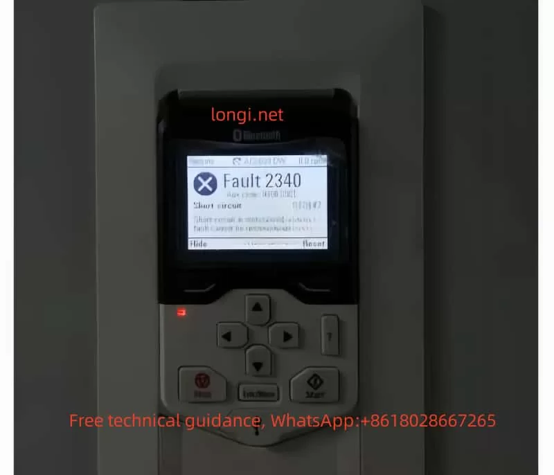
The ABB ACS880 series inverters are widely used in industrial applications due to their high performance and reliability. However, issues can arise, especially when driving high-power motors. One such challenging fault is **Fault 2340**, which is related to motor cable or motor short circuits and IGBT module malfunctions. This article will analyze the potential causes of Fault 2340 and provide a troubleshooting guide to resolve it.
1. Fault Symptoms
In a real-world scenario, an ABB ACS880 inverter was used in a common DC bus system to drive a 1150HP motor. During startup, Fault 2340 occurred intermittently—about two to three times out of ten attempts. After thorough inspection, the motor insulation was found to be normal, ruling out motor and motor cable issues as the root cause.
2. Analysis of Causes for Fault 2340
(1)Motor Cable Insulation Issues: While the motor insulation was normal in this case, it’s essential to consider the possibility of phase-to-phase or phase-to-ground insulation issues in the motor cables, which could lead to Fault 2340. Though this is less likely, it should not be overlooked during troubleshooting.
(2)IGBT Module and Gate Driver Board Issues: The IGBT module is a critical component in the inverter. Faulty signals from the gate driver board of the IGBT module are a common cause of Fault 2340. This issue has a high probability and often requires replacing the IGBT module to resolve.
(3)Connection Issues Between IGBT Module and Interface Board**: If the ribbon cables connecting the IGBT module to the interface board are damaged or have high resistance, Fault 2340 may occur. This issue is moderately probable and should be addressed by thoroughly inspecting the connections.
(4)Interface Board Fault**: The interface board transmits control signals to the IGBT module. A malfunctioning interface board can also trigger Fault 2340. This issue is moderately likely and should be considered if other checks do not resolve the fault.
(1)Initial Inspection**:
– Use a multimeter to measure the diode characteristics between the inverter output terminals (U, V, W) and the DC bus terminals (R+, R-) to ensure they match expected values.
– Perform an insulation test on the motor and its cables to confirm there are no short circuits or grounding issues.
– Inspect the inverter for signs of moisture, condensation, or burn marks.
(2)Component Replacement**:
– If initial inspections reveal no issues, consider replacing the AINT board (interface board) to see if the fault is resolved.
– If the fault persists, disassemble the inverter and replace the IGBT module. During this process, carefully inspect all connections to ensure there are no loose or broken wires.
(3)Further Diagnosis**:
– If replacing the IGBT module and interface board does not resolve the issue, check and replace the current sensors and brake chopper IGBT.
– Throughout the process, handle all components with care, especially during reassembly, to prevent introducing new issues, such as poor connections or short circuits.
4. Conclusion
Fault 2340 in the ABB ACS880 inverter is a complex issue with multiple potential causes, ranging from motor cable insulation problems to IGBT module failures. Effective troubleshooting requires a thorough understanding of the inverter’s components and a methodical approach to diagnosing and repairing the fault. By following the steps outlined in this guide, technicians can systematically address and resolve Fault 2340, ensuring the reliable operation of the inverter.
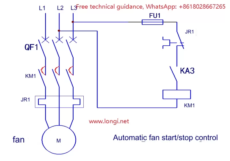
The user went to a hardware and electrical store to buy a thermometer for automatic temperature control of the material tank in the production workshop. The control requirements put forward by the user are: when the temperature of the material tank is as low as 25 º C, start the boiler fan to heat it up; when the temperature of the material tank rises to 32 º C, stop the fan. The temperature is not required to be precisely controlled at one point, but it can be roughly maintained between 25 º C and 32 º C. In this way, the fan does not need to be started frequently and run for a long time, and the power saving effect will be very good. It is said that after searching several electrical and mechanical stores, no suitable temperature control meter can be found. If it can be solved here, it doesn’t matter if the price is a little higher, and five or six units can be purchased at once.
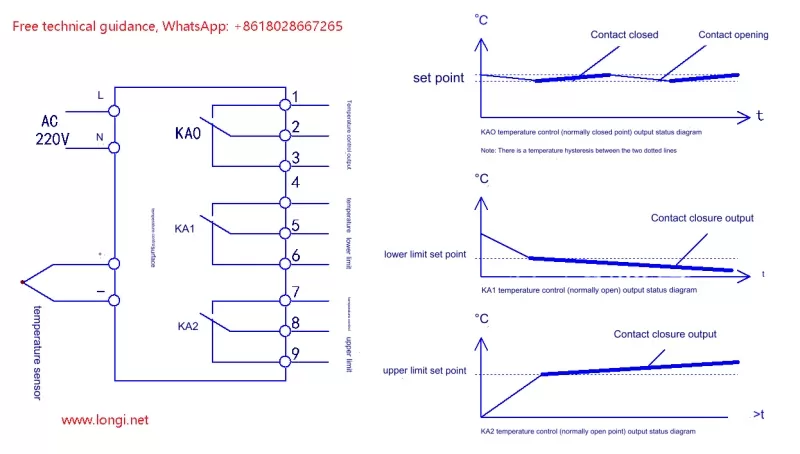
The father and son run the hardware and electrical store. The father is an old electrician, and the son is a student of the Department of Mechanical and Electrical Engineering, with top grades. The father and son were excited and decided to make this deal. The temperature controllers in the store generally have the following functions, see the wiring diagram below:
Figure 1: Temperature control meter wiring and three sets of contact output status diagram
From the wiring diagram, the temperature controller has three groups of output control contacts. KA0 is the control temperature output. If its normally closed point is used as the control output, the contact closing and opening action area is near the temperature setting point. For example, if the setting point is 25 º C, when the measured temperature rises to 25 º C, the normally closed contact is disconnected, and when the measured temperature drops to 23 º C, the contact is closed. This control method belongs to “point” control. The action of the relay tracks a temperature setting point. Although in order to avoid frequent switching at one point, there is often a temperature hysteresis value in the middle, such as 2 º C between 23 º C and 25 º C. Some models have this hysteresis fixed, while others are adjustable, but the temperature difference adjustment range is not too large. Obviously, the control output contact of KA0 cannot meet the control requirements put forward by users.
Let’s look at the output contact of KA1, which is the lower limit control output. It is also output based on a “temperature point”. When the measured temperature reaches the preset lower limit, KA1 will act. As long as it is within the lower limit, KA1 will maintain the output. Only when the measured temperature is higher than the lower limit setting point, KA1 will lose power and the contact will be released. The control requirements cannot be achieved by relying solely on the control contacts of KA1. The output contact of KA2 is the upper limit setting point. Its control principle is the same as that of KA1. It can also be regarded as a “point” control and cannot complete the control task independently.
My son suddenly had an idea: Is it possible to combine the lower limit and upper limit control outputs to meet the control requirements proposed by the user?
Dad nodded approvingly: Okay, I thought so too, let’s try to analyze it.
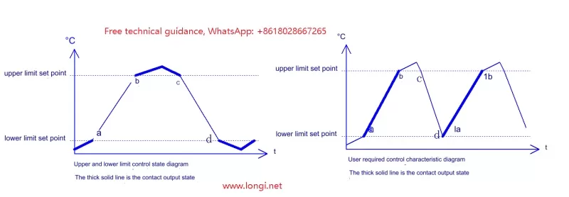
See the following control state diagram of KA1 and KA2 output combination and user control requirement diagram:
Figure 2: Upper and lower limit control states and user required control characteristic diagram
My son said: By connecting the normally closed points of the two relays KA1 and KA2 in series, the fan can be powered on and operated in the area where the two relays are not operating. That is, the fans in sections a and b in the figure can be powered on and operated. Doesn’t this meet the requirements?
Dad said: It seems not to work. The fan is also powered in sections c and d. The fan is powered and running most of the time. The fan stops only when it is outside the upper and lower limits. It still doesn’t work to use the two contacts directly. The user’s requirements are shown in the right figure of Figure 2. Only the thick line segments (a, b/1a, 1b) in the right figure are the time for the fan to run. When the detected temperature reaches the lower limit, the fan runs, and when it reaches the upper limit, the fan stops; then the temperature drops and reaches the lower limit again, the fan starts running again. The fan does not run at one “point”, but only runs on “segments” a and b, achieving a good power saving effect.
My son said: I didn’t notice the c and d segments in the left figure. It’s not possible. But we can use the upper and lower limit contact outputs and add an external control circuit to achieve it. This additional circuit should not be difficult to make.
The father wanted to test his son’s level, so he said: How about this, let’s both make an external control circuit, and see who’s circuit is simpler and more reasonable, and then we’ll use their circuit, okay?
The son knew that his father wanted to test his ability and it was also a small challenge for him. He thought that since he had worked on some complicated electromechanical control circuits, this small circuit should be no problem for him. So he readily agreed.
It seems to be a simple thing to think about, but in practice, this small function is not so easy to achieve. It seems that it cannot be completed with two additional relays, and the circuit is too complicated to use three relays. According to my father’s idea, it should be possible to achieve it with two additional relays. It seems that it cannot complete the task if one contact of KA1 and KA2 is used.
The son spent half a day drawing several diagrams, optimizing and simplifying the circuit, and finally succeeded through wiring tests. However, the analysis from the control principle was a bit confusing. The father frowned and thought about it at first, but suddenly grabbed a pen and drew a wiring diagram in no time. Without wiring tests, he announced that the circuit would definitely work.
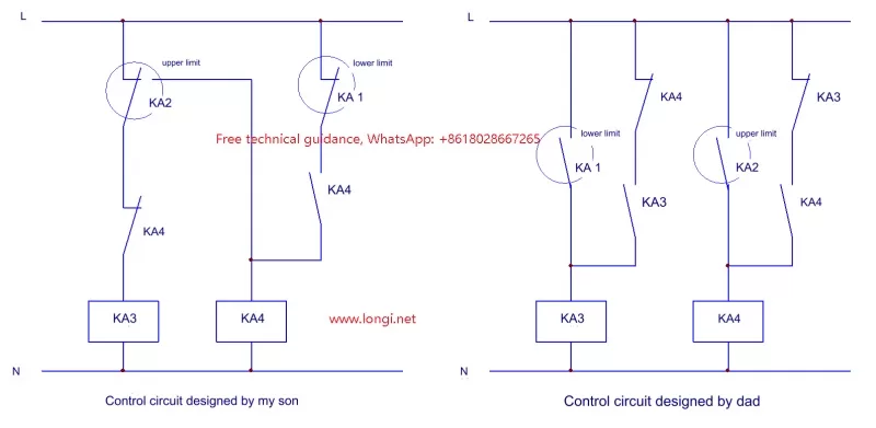
The control circuit diagram made by the father and son is as follows:
In the figure, KA1 and KA2 are the upper and lower limit signal output relays inside the temperature control meter, KA3 and KA4 are external relays, and KA3 provides control signal output. The control circuit designed by my son uses the normally open and normally closed contacts of the upper limit relay, the normally closed contacts of the lower limit relay, and two sets of contacts of KA4. The control process is as follows: After the equipment is powered on, the normally closed contact circuit of KA2 and KA4 provides power to the KA3 coil, KA3 is energized, the fan runs, and the discharge tank begins to heat up; when the temperature reaches the upper limit, the normally closed point of KA2 is disconnected, the normally open point is connected, KA3 loses power, and at the same time KA4 is energized for self-protection, the fan stops, and the discharge tank begins to cool down; due to the self-protection effect of KA4, when the temperature drops below the upper limit, KA4 maintains an energized state through the normally closed point of KA1 and its own self-protection contact, and KA3 maintains a de-energized state, and the temperature of the discharge tank continues to drop until it reaches the lower limit of the temperature, the KA1 lower limit relay is activated, the KA4 self-protection circuit is disconnected, KA4 loses power, KA3 is energized again, and the fan runs.
The control circuit designed by my father seems to be simpler. The circuit is clear in principle and is more convenient for analyzing the control process: when the temperature of the unloading tank reaches the lower limit, KA3 is energized and forms a self-protection (self-locking) circuit through the normally closed point of KA4 and the normally open point of KA3, and the fan runs; when the temperature reaches the upper limit, the normally open point of the upper limit relay KA2 is connected, KA4 is energized, and while disconnecting the self-locking circuit of KA3, it forms its own self-locking circuit through the normally closed point of KA3 and the normally open point of KA3. KA4 remains energized, KA3 remains de-energized, and the fan stops; when the temperature drops to the lower limit of the temperature, the relay KA1 is activated, KA3 is activated, and while disconnecting the self-locking circuit of KA4, KA3 forms its own self-locking circuit, and the fan starts running again.
The focus of control requirements is to meet two conditions:
1. Once KA3 and KA4 are powered, they can be self-protected (self-locked);
2. When two relays are powered on for self-protection, the self-protection circuit of relay B must be disconnected to make it lose power. The same is true in reverse.
This control method is not conventional temperature point control, but temperature range control, which can be regarded as a special application.
Both the son’s and the father’s circuits can accomplish the task, and use the same number of contacts, but the father’s circuit is easier to understand and more classic. The son’s circuit also accomplishes the task well, which is rare.
Dad said: I thought of these two conditions, and based on these conditions, I formed this circuit in the computer. It was a waste of effort before the logical relationship of the circuit was clear.
Although the son has figured out the circuit, it seems that his father is still better in terms of circuit routing and principle analysis. His father’s circuit is more “smooth”, while my own circuit is a bit tortuous. When you make a circuit yourself, you should be better at analyzing the logical relationship and take a “smooth” path to make the circuit more optimized and reasonable.
The fan control wiring diagram is as follows:
In the figure, KA1 and KA2 are the upper and lower limit signal output relays inside the temperature control meter, KA3 and KA4 are external relays, and KA3 provides control signal output. The control circuit designed by my son uses the normally open and normally closed contacts of the upper limit relay, the normally closed contacts of the lower limit relay, and two sets of contacts of KA4. The control process is as follows: After the equipment is powered on, the normally closed contact circuit of KA2 and KA4 provides power to the KA3 coil, KA3 is energized, the fan runs, and the discharge tank begins to heat up; when the temperature reaches the upper limit, the normally closed point of KA2 is disconnected, the normally open point is connected, KA3 loses power, and at the same time KA4 is energized for self-protection, the fan stops, and the discharge tank begins to cool down; due to the self-protection effect of KA4, when the temperature drops below the upper limit, KA4 maintains an energized state through the normally closed point of KA1 and its own self-protection contact, and KA3 maintains a de-energized state, and the temperature of the discharge tank continues to drop until it reaches the lower limit of the temperature, the KA1 lower limit relay is activated, the KA4 self-protection circuit is disconnected, KA4 loses power, KA3 is energized again, and the fan runs.
The control circuit designed by my father seems to be simpler. The circuit is clear in principle and is more convenient for analyzing the control process: when the temperature of the unloading tank reaches the lower limit, KA3 is energized and forms a self-protection (self-locking) circuit through the normally closed point of KA4 and the normally open point of KA3, and the fan runs; when the temperature reaches the upper limit, the normally open point of the upper limit relay KA2 is connected, KA4 is energized, and while disconnecting the self-locking circuit of KA3, it forms its own self-locking circuit through the normally closed point of KA3 and the normally open point of KA3. KA4 remains energized, KA3 remains de-energized, and the fan stops; when the temperature drops to the lower limit of the temperature, the relay KA1 is activated, KA3 is activated, and while disconnecting the self-locking circuit of KA4, KA3 forms its own self-locking circuit, and the fan starts running again.
The focus of control requirements is to meet two conditions:
1. Once KA3 and KA4 are powered, they can be self-protected (self-locked);
2. When two relays are powered on for self-protection, the self-protection circuit of relay B must be disconnected to make it lose power. The same is true in reverse.
This control method is not conventional temperature point control, but temperature range control, which can be regarded as a special application.
Both the son’s and the father’s circuits can accomplish the task, and use the same number of contacts, but the father’s circuit is easier to understand and more classic. The son’s circuit also accomplishes the task well, which is rare.
Dad said: I thought of these two conditions, and based on these conditions, I formed this circuit in the computer. It was a waste of effort before the logical relationship of the circuit was clear.
Although the son has figured out the circuit, it seems that his father is still better in terms of circuit routing and principle analysis. His father’s circuit is more “smooth”, while my own circuit is a bit tortuous. When you make a circuit yourself, you should be better at analyzing the logical relationship and take a “smooth” path to make the circuit more optimized and reasonable.
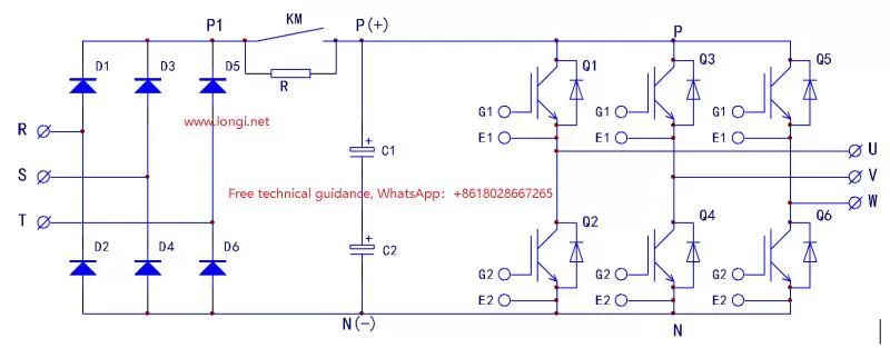
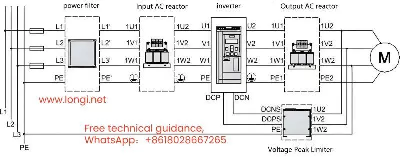
The main circuit of the inverter is a voltage-type, AC-DC energy conversion inverter. Since there is a large-capacity capacitor energy storage circuit between the rectifier and inverter circuits, and the voltage across the capacitor cannot change suddenly, in the initial power-on stage, the capacitor device is equivalent to a “short circuit”, which will form a huge surge charging current, which will cause a large current impact on the rectifier module and cause it to be damaged, and will also cause the air circuit breaker connected to the inverter power supply end to trip due to overcurrent.
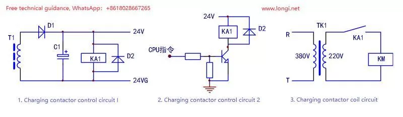
The conventional processing method is to connect a current limiting resistor and a charging contactor (relay) in series between the rectifier and the capacitor energy storage circuit. The control of the capacitor charging process is as follows:
When the inverter is powered on, the charging resistor first limits the current of the capacitor to suppress the maximum charging current. As the charging process extends, the charging voltage gradually builds up on the capacitor. When the voltage amplitude reaches about 80% of 530V, two control processes occur. One is that the switching power supply circuit of the inverter starts to oscillate. The 24V output of the switching power supply directly drives the charging relay, or the relay connects the coil power supply circuit of the charging contactor. The charging contactor (relay) is closed. When the charging current limiting resistor is short-circuited, the inverter enters the standby working state. After a certain voltage is established on the capacitor, its charging current amplitude is greatly reduced, and the closing/switching current of the charging contactor is not too large. After that, the power supply of the energy storage capacitor circuit and the inverter circuit is supplied by the closed contactor contacts, and the charging resistor is short-circuited by the normally open contact of the contactor. The second is that as the charging voltage on the capacitor is established, the switching power supply starts to oscillate, and the CPU detects the voltage amplitude signal sent by the DC circuit voltage detection circuit, determines that the charging process of the energy storage capacitor has been completed, and outputs a charging contactor action instruction. The charging contactor is powered on and closed, and the capacitor charging process ends.
The common main circuit forms of the inverter and the charging contactor control circuit are shown in the figure below:
Figure 1: Common types of inverter main circuits
Figure 2: Control circuit of charging contactor
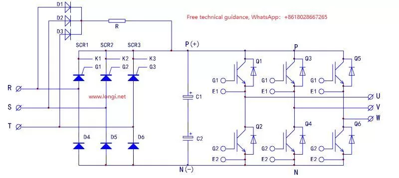
For some inverters and high-power inverters, the rectifier circuit often adopts a three-phase half-controlled bridge circuit, that is, the lower three arms of the three-phase rectifier bridge are rectifier diodes, and the upper three arms use three unidirectional thyristors, using thyristors as “contactless switches” to replace charging contactors. This saves installation space and improves circuit reliability. The circuit form is shown in the figure below:
Figure 3: Control circuit of charging contactor
Although the charging contactor is omitted, the working principle is the same, but the control circuit is different. During the power-on period of the inverter, D1 ∽ D6 is used for rectification, and R is used for current limiting to charge C1 and C2. When the charging process is close to the end, the CPU outputs the opening instruction of the three thyristors SCR1 ∽ SCR3, and the control circuit forces the three thyristors to conduct. The power-on pre-charging circuit composed of D1, D2, D3, and R is used. SCR1 ∽ SCR3 and D4, D5, and D6 form a three-phase rectifier bridge. At this time, the thyristor is in a fully conductive state, which is equivalent to a rectifier diode.
The opening of the thyristor requires two conditions: 1. The positive voltage between the anode and the cathode; 2. A trigger current loop is formed between K and G. The circuit is connected to the three terminals of the AC input power supply to provide unidirectional controlled rectification. During the three positive half-wave voltages of the three-phase AC power, if the trigger current is formed at the same time, the three thyristors can be opened. The first condition has been formed naturally, and the second condition is sufficient to control its opening.
To put it simply, as long as a trigger current (pulse or DC) is provided to the thyristor during the period when the thyristor is subjected to a forward voltage – when the AC voltage passes through zero, the thyristor can be turned on well during the positive half-wave of the AC power and rectify the input AC voltage (just like a diode). The simplest trigger circuit is to introduce a resistor from the anode to the G pole, and during the positive half-wave of the AC power (after the zero point), the trigger current is synchronously introduced to the thyristor to turn on the thyristor. For example, the main circuit form of Dongyuan 300kW inverter is the same as Figure 3, and the trigger circuit is relatively simple:
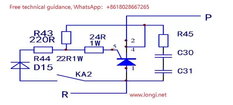
Figure 4: SCR trigger control circuit 1
Figure 4 is one of the thyristor trigger circuits. The other two trigger circuits are the same. The components R45, C30, C31 and other components connected in parallel at the anode and cathode of the two thyristors are peak voltage absorption networks to provide overvoltage protection for the thyristors. The KA2 contact, D15, R44, and 24R form a trigger current path. The function of D15 is to rectify the input voltage half-wave to prevent the thyristors G and K from being subjected to the impact of reverse trigger voltage/current. R44 and 24R are current limiting resistors to limit the peak trigger current and protect the safety of the thyristors. R43 is a noise elimination resistor to increase the reliability of the thyristor operation.
When the CPU issues a thyristor on command, relay KA2 is powered on and closed, a positive half-wave voltage is input, rectified by D15, limited by R44 and 24R, flows into the G pole of the thyristor, and flows out from the K pole, forming a trigger current path, and the thyristor is turned on. The thyristor in the circuit is not in the voltage regulation working area, the conduction angle is the largest, and it is in the “full conduction state”, just like a switch device, only in the two states of conduction and cutoff, without the third state of phase shift (voltage regulation). This is where attention needs to be paid. Therefore, the control circuit is different from the conventional phase shift control circuit and is relatively simple.
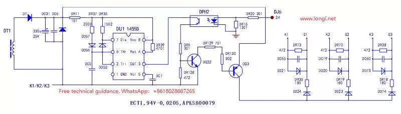
A slightly more complex thyristor control circuit, such as the trigger circuit of the Delta 37kW inverter thyristor, is shown in the figure below:
Figure 5: SCR trigger control circuit 2
After rectification and filtering by an independent power supply winding of the switching power supply, it is used as the power supply for the thyristor trigger circuit. The control circuit consists of the NE555 time base circuit, the DPH2, DQ22, DQ3 trigger pulse on/off circuit, and the D and R three-way trigger flow circuit. After the switching power supply works, the NE555 time base circuit is connected to a multi-resonance oscillator and is powered on. Whether the oscillation pulse output from pin 3 is sent to the three trigger circuits of the subsequent stage depends on the command control of the CPU. The command signal of the CPU is introduced to the input side of the photocoupler DPH2 through the 24th pin of the control wiring terminal DJ8. When the transistor on the output side of the optocoupler is turned on, the pulse signal of the NE555 oscillator is sent to the D and R trigger circuit loop of the subsequent stage through the transistors DQ22 and DQ3. After the CPU issues the thyristor opening command, the three devices DPH2, DQ22, and DQ3 are always in the on state, and the trigger pulse is always added to the G and K of the three thyristors. The peak trigger current is about 100mA.
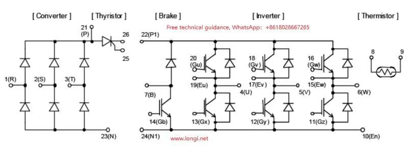
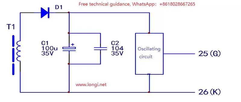
In addition, in the Panasonic and Fuji small power inverter models, another form of main circuit structure is used to complete the initial charging control of the main circuit capacitor. This is the internal circuit structure diagram of the 7MBR35SD120 integrated power module. The circuit is shown in Figure 6:
The difference of the circuit is that a controllable device is added after the three-phase rectifier bridge. A charging resistor must be connected in parallel to the terminals 21 and 26. After a certain charging voltage is established on the main circuit capacitor, a trigger current is input from terminals 25 and 26, then the thyristor is turned on and the inverter enters the standby working state.
The control circuit is generally powered by an independent 24V winding of the switching transformer to obtain control power with a “floating ground”. The control circuit is mostly an oscillation circuit, which increases the pulse trigger current of the thyristor device. The oscillation circuit is not a conventional phase-shift trigger circuit, but provides high-frequency/density random trigger pulses to put the thyristor in a fully conductive state. The thyristor here, under the action of high-density trigger impulses, is like a switch “turned to the on position”. There is no actual surveying circuit on hand for the trigger circuit of this model, so we can only draw a simple diagram based on the circuit structure for reference.
Figure 6: 7MBR35SD120 integrated power module
Figure 7: thyristor trigger circuit of 7MBR35SD120S module
A factory has a 5.5 kW submersible pump. To facilitate water volume adjustment and energy-saving operation, an electrician proposed using a VFD to drive the pump.
The task was taken on by Mr. Zhang, a friend of the electrician. For safety, Mr. Zhang selected a 7.5 kW VFD from a reputable brand. This brand’s VFDs are widely used in various industries such as plastics, chemicals, and wood processing without significant issues, indicating decent quality. The VFD control box was installed in the boiler room, with power sourced from the workshop distribution panel. The three-phase voltage balance was excellent, maintaining within 380V ±5%. During the trial run, the VFD did not need to operate at full speed, running around 30Hz with the working current at half of the VFD’s rated current. Mr. Zhang was confident that the VFD would operate safely for a long time.
However, three days later, the factory’s electrician called Mr. Zhang, reporting that the VFD had stopped, and the control panel was unresponsive, indicating no power. Surprised, Mr. Zhang visited the site and confirmed the issue. Assuming a quality problem with the VFD, he replaced it with another 7.5 kW VFD from the supplier and sent the defective one for repair.
This time, the VFD failed after just a day and a half. Frustrated, Mr. Zhang called the supplier to complain and replaced the VFD with another brand. He again checked the operating voltage and current, which were similar to the initial installation, indicating no issues with the pump or power supply. Mr. Zhang concluded that the first batch of VFDs might have had quality defects and hoped the new brand would solve the problem.
Unexpectedly, the newly installed VFD also failed within hours, with the factory’s electrician calling Mr. Zhang again. The recurring issue led to reprimands from the factory boss to the electrician, who then passed the blame to Mr. Zhang. Baffled, Mr. Zhang inspected the three faulty VFDs. He found that two had open circuits between the R and P1 (external brake resistor terminal), possibly due to damaged charging resistors, which indicated rectifier circuit issues. The third VFD had a short circuit between R and S, suggesting a failed rectifier module. However, the inverter modules in all three VFDs were intact. The damages seemed to result from power surges, not load-related issues, as the three-phase supply voltage and input current were normal. Having worked with VFDs for several years, Mr. Zhang found this problem unprecedented.
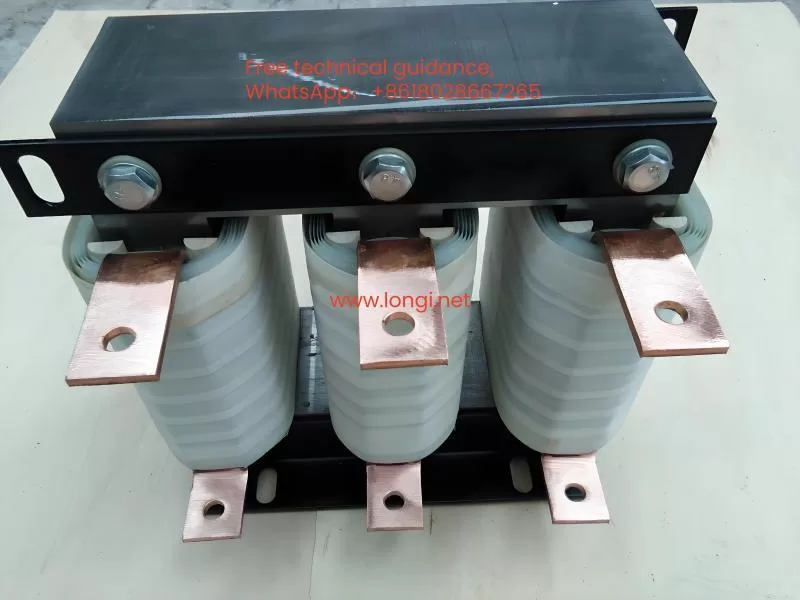
In desperation, Mr. Zhang called his friend, electrician Mr. Li, for advice. Mr. Li suggested installing a three-phase input reactor before the VFD’s power terminals to solve the problem.
Mr. Zhang inquired about the cause of the failures. Mr. Li explained three potential reasons related to the power supply:
1. The submersible pump continued to operate after work hours for employee showers, meaning a 630 kVA transformer supplied a 7.5 kW VFD, causing a significant capacity disparity. The VFD’s input current contained high harmonic components, generating large rectifier inrush currents that damaged the rectifier module and charging resistor during startup.
2. The workshop distribution panel might have parallel capacitor compensation cabinets. The start and stop of large motors (above 100 kW) and the switching currents of capacitors created harmful voltage spikes and inrush currents, impacting the VFD.
3. The same power line might have other large VFDs, soft starters, or DC speed controllers. The nonlinear rectifier currents from these devices severely distorted the power supply waveform, increasing harmful harmonics and deteriorating power quality.
Mr. Li noted that input reactors, often depicted in VFD wiring diagrams, are frequently omitted during installation to save costs, leading to such issues.
Mr. Zhang didn’t have ready-made three-phase reactors and needed an immediate solution. Mr. Li suggested using XD1 series chokes from old capacitor compensation cabinets as reactors, which could suppress inrush currents effectively. Mr. Zhang contacted several suppliers but learned that most manufacturers had stopped producing these chokes.
Under pressure, Mr. Zhang reached out to Mr. Li again, demanding a solution. Mr. Li, while having lunch, suggested using current transformers (CTs), which Mr. Zhang likely had. Any CT, regardless of size, with a rated current of 5A, could be used. CTs with more winding turns (e.g., 50/5) would offer better inrush current suppression and filtering but might have a higher voltage drop. Conversely, CTs with fewer turns (e.g., 250/5) would have a smaller voltage drop but less effective smoothing. Depending on the VFD’s rated current, Mr. Li recommended using three CTs per phase or two if the running current was around 7A. CTs would provide better inductance and performance than XD1 chokes.
After installing CT-based “input reactors,” the VFD’s input current became stable, reducing harmonics and voltage spikes, ensuring safer operation.
Months later, Mr. Zhang checked with the factory electrician, who confirmed that the VFD had been operating normally. Mr. Zhang realized the VFD failures were due to power supply issues, not the VFD quality. He felt vindicated and teased the electrician about owing him a drink for resolving the issue.
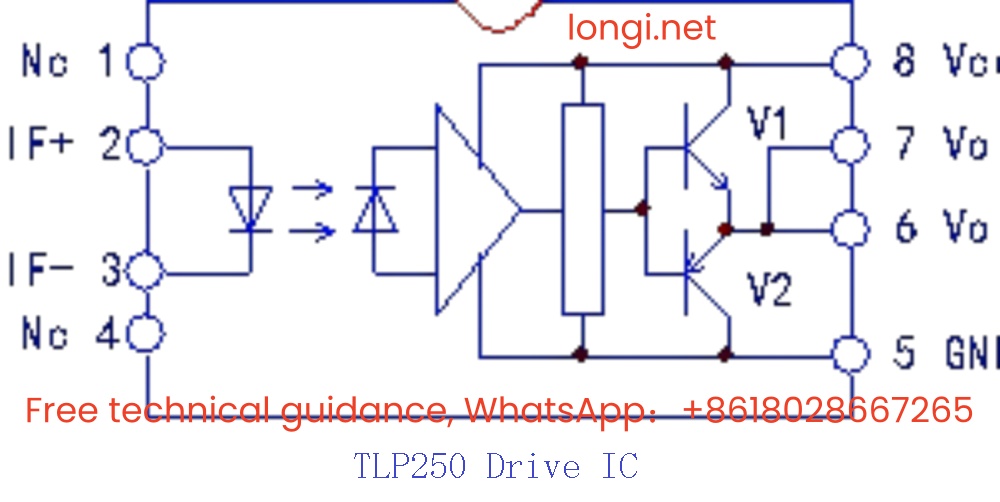
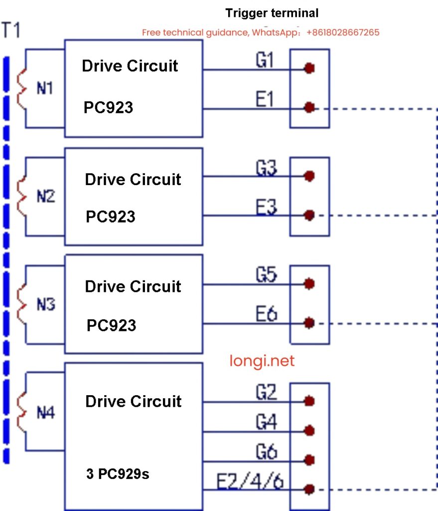
1. The difference between various types of driver ICs:
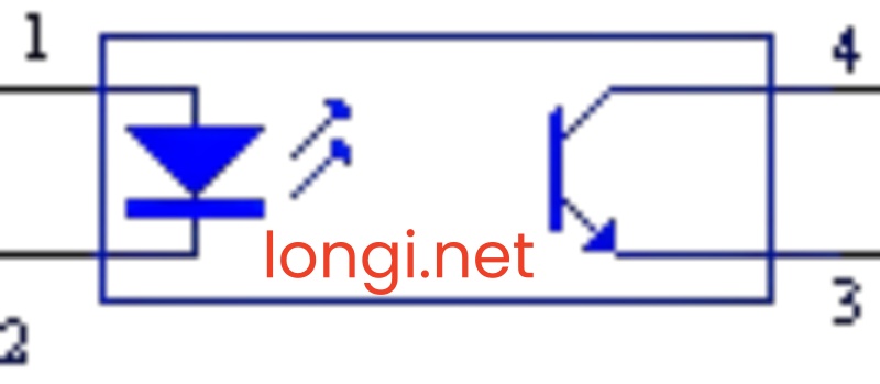
The core component of the inverter drive circuit is the driver IC, and the commonly used models are TLP250, A3120, PC923, PC929, A316J, etc. The driver IC is essentially a type of optocoupler device. The purpose of using optocouplers is to achieve isolation of different power supply circuits on the input and output sides of the coupling, and to ensure that the output side has a certain power driving capability, which has both electrical isolation and power amplification.
Ordinary four-wire end optocoupler devices, such as PC817, have an internal circuit consisting of an input light-emitting diode and an output photosensitive transistor. After the input current (typical application value 5-10mA) is passed through the input side , the output side transistor generates excited photoelectrons and conducts. This type of optocoupler is mainly used for the transmission of switching signals, such as the digital signal control terminal of the inverter.
As an optocoupler device of the driver IC, its structure is slightly more complicated than that of PC817. The output stage is mostly composed of emitter output to the complementary amplifier, such as TLP250, A3120, PC923, etc. The output stage is composed of two-stage emitter complementary circuits, V1 and V2. When V1 is turned on, the VCC positive supply voltage is added to the gate-emitter junction of the IGBT through the output pins 6 and 7, providing the driving current for the IGBT to turn on. If the gate-emitter junction of the IGBT is regarded as a capacitor, the V1 conduction provides the charging current of the gate-emitter junction capacitor of the IGBT to turn it on; and when V2 is turned on, the output pins 6 and 7 are pulled to the GND ground level or the negative supply voltage, providing a charge discharge channel for the gate-emitter junction capacitor of the driven IGBT, so that it is quickly cut off. During work, V1 and V2 are alternately turned on to implement the on and off control of the IGBT. It should be noted that the power supply for this drive circuit often uses a positive and negative dual power supply of +15V and -7.5V to enhance its control ability.
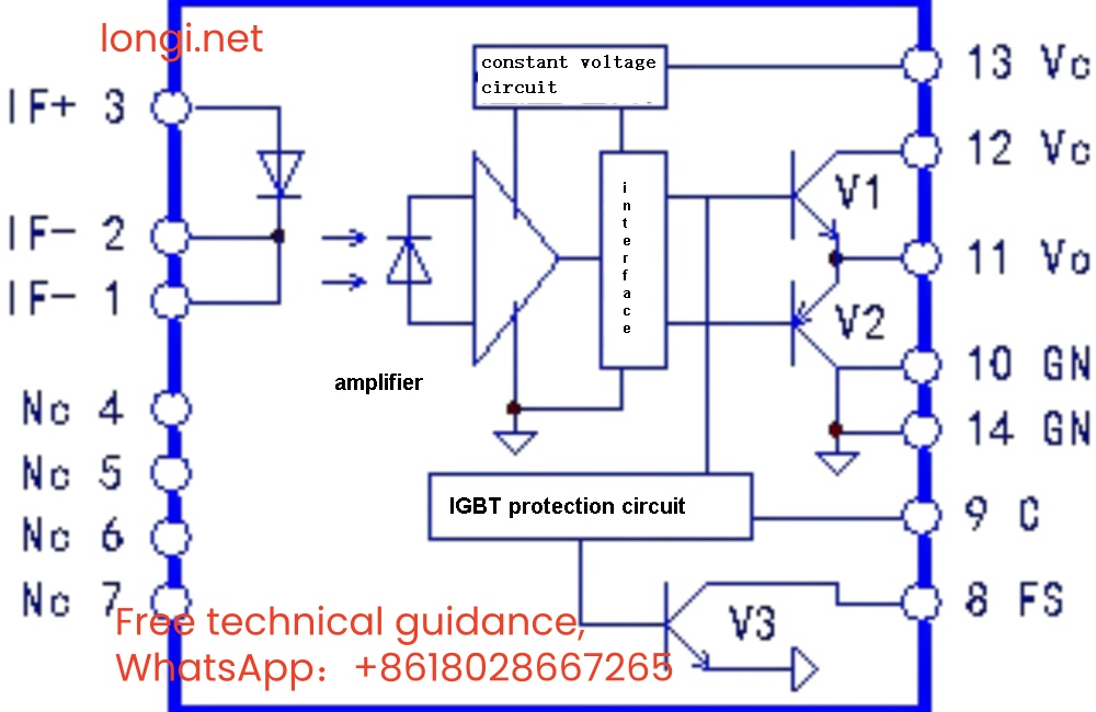
PC929 adds IGBT protection circuit, also known as IGBT conduction tube voltage drop detection circuit, based on the circuit structure of TLP250, A3120, PC923, etc., which is mainly responsible for the rapid protection of IGBT from overcurrent and short circuit. As we all know, in the U, V, W output circuit of the inverter, two or three current transformers are connected in series (the current signal is collected by the Hall element and processed by the amplification circuit), and the output signals are processed into analog and switch signals by the back-stage circuit respectively, and sent to the CPU for current display, output control, automatic speed control and current limiting control and overload protection during startup and operation. However, the current transformer circuit often has a large time constant and cannot implement μs -level rapid protection for IGBT. In fact, the implementation of overload and short circuit protection for IGBT depends on driver ICs such as PC929 and A316J to a certain extent.
Because the tube voltage drop when the IGBT is turned on actually reflects the working state of the IGBT, the overcurrent detection of the IGBT can be implemented by using the IGBT’s energy-conducting tube voltage drop signal, which can effectively implement the rapid overcurrent protection of the IGBT. The IGBT tube is an organic combination of a two-stage device and a field-effect device. The collector and the emitter form an output current path and have a certain conduction internal resistance. When the IGBT works within the rated current, the normal conduction tube voltage drop should be less than 3V. When the overcurrent is nearly 2 times, the overload current forms a large voltage drop on its conduction internal resistance, causing the tube voltage drop to rise to about 7V. Since the overload capacity of electronic devices is poor, the overload time allowed is short, and the faster the protection action, the better. Detecting the IGBT’s conduction tube voltage drop signal to cut off and protect the IGBT has become the most effective and widely used method in the inverter drive circuit.
Compared with PC923, PC929 (pictured above) has an additional IGBT protection circuit. Pin 9 is connected to the C and E poles of the driven IGBT together with the external components to detect the IGBT conduction tube voltage drop signal. When the tube voltage drop signal rises to above 7V due to overcurrent, the internal triode V3 of pin 8 is turned on, and the OC and SC signals are isolated by the external optical coupler and sent to the CPU. The inverter reports the OC signal and shuts down for protection. (For details, please refer to the article “Repair of PC923 and PC929 drive circuits”)
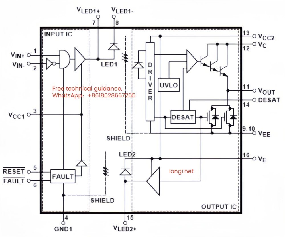
However, it can be seen from the circuit structure of PC929 that V3 of the OC alarm circuit is directly electrically connected to the output side circuit, which is the strong current side. The OC signal can only be sent to the CPU through optocoupler isolation. Assuming that the optocoupler that transmits the OC signal is also integrated into the driver IC, the OC signal output pin of the driver IC can be directly connected to the CPU pin. Then the A316J in the driver IC can complete this task.
The internal circuit structure of A316 is shown in the figure below. The PWM pulse signal from the CPU is input through pins 1 and 2, isolated by the internal photocoupler LED1, the interface circuit and the power output circuit, and output from pin 11 to drive the IGBT; the external components at pins 14 and 16 and the internal circuit constitute the IGBT tube voltage drop detection circuit. When the IGBT protection circuit is activated, the LED2 photocoupler transmits the OC signal to the input side, which is output from pin 6 and sent to the CPU.
Compared with other driver ICs, A316J has the following two features:
(1) The input side is not a light-emitting diode, but a digital gate circuit. It does not need to draw a large original drive circuit from the signal source. The input impedance is high and it is easy to connect directly to the CPU pin, eliminating the intermediate drive circuit link.
(2) After the OC signal fault occurs, there is a fault lock function, which blocks the transmission of the pulse signal. Only after a low-level reset signal is input from pin 5, can the fault lock state be released and the pulse transmission path be opened. Therefore, A316J also has a fault reset function.
In this sense, A316 is an integrated driver IC with the most complete control functions.
2. Methods for removing OC fault alarm
During maintenance, we often need to disconnect the drive circuit from the main circuit for separate inspection. At this time, the OC fault alarm function of the drive circuit will cause us a little trouble. When the drive board is powered on separately, the operation panel often reports an OC fault, making it impossible for us to detect whether the drive circuit is normal.
It is necessary to take corresponding measures to release the OC fault alarm function of the drive circuit to facilitate the inspection of whether the drive circuit can transmit six-channel drive pulses normally.
In the drive circuit, PC923 and PC929 often appear in pairs, and PC929 is responsible for detecting the voltage drop of the lower three-arm IGBT conduction tube, and reports the OC signal to the CPU when a fault occurs. When the drive board is disconnected from the main circuit IGBT, it is equivalent to the IGBT open circuit. Once the start signal is sent, PC929 will send an OC signal to the CPU.
pulse trigger terminals E1 – E6 (dashed lines in the figure below) to artificially create the false appearance of “normal opening” of the three-arm IGBT in the inverter circuit. PC929 no longer returns OC signal to the CPU, so the CPU outputs six pulse signals to six driver ICs, so that you can check whether the drive circuit is normal.
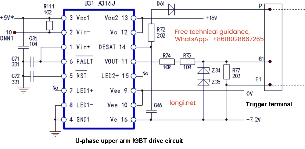
The A316J driver IC can also detect the voltage drop of the upper three-arm IGBT and report the OC signal. See the figure below:
By short-circuiting the trigger terminals P and E1, the “conditions” for turning on the IGBT are artificially created, thus releasing the OC fault detection and alarm function of A316J.
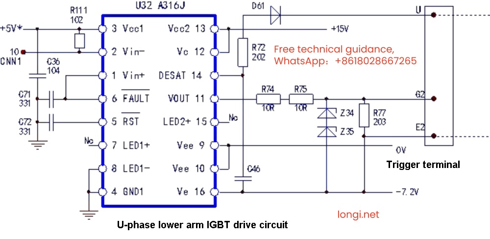
The method of removing the OC alarm function of the three-arm IGBT drive circuit of A316J is the same as above. See the figure below:
The driving circuit of the U-phase lower arm IGBT can short-circuit the U and E2 contact terminals, thereby releasing the IGBT tube voltage drop detection and OC signal alarm functions.
There are two points to note:
(1)For the detection of the voltage drop of the lower three arms or the lower three arms IGBT tubes separately, the trigger terminals of the upper three arms or the lower three arms can be short-circuited to release the OC alarm function. For the detection of the voltage drop of all six IGBT tubes, only the trigger terminals of the upper three arms IGBT can be short-circuited, and the OC alarm of the lower three arms can only be released by using a fine needle to pick up the 6th pin of A316; after checking that there is no problem with the upper three-arm drive circuit, remove the short-circuit line, pick up the 6th pin of the upper three-arm drive IC, short-circuit the trigger terminal of the lower three-arm drive circuit, and check whether the lower three-arm drive circuit is normal;
(2)If the trigger terminal has two pins, only G2 and E2, you should find the cathode of diode D61 from the 14 peripheral circuit of A314J, short-circuit it with E2, and release the OC alarm function.
Most of the maintenance of the inverter is the maintenance of the drive circuit. After the drive circuit is repaired, the power-on test of the inverter circuit must be cautious! ! You should use measures such as series light bulbs, 2A fuses, and DC low voltage. After confirming that the inverter circuit is fault-free, restore the 530V DC power supply.