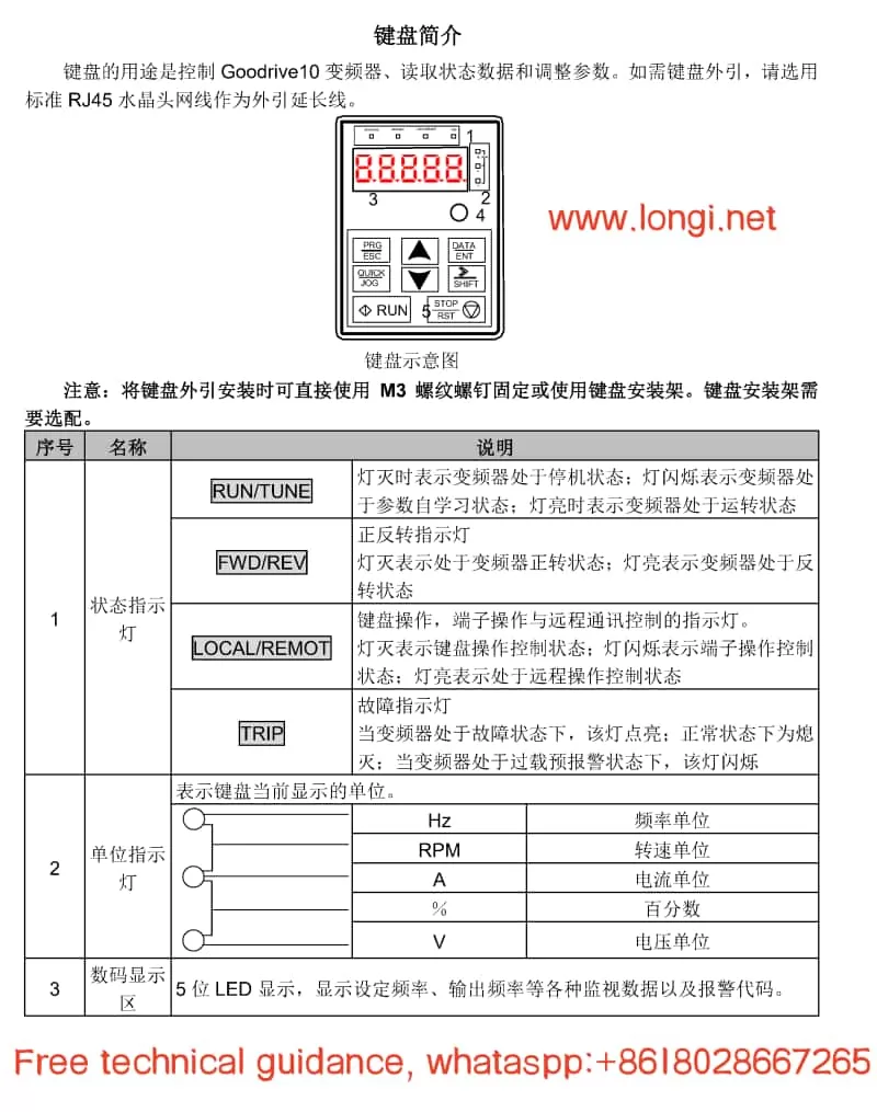
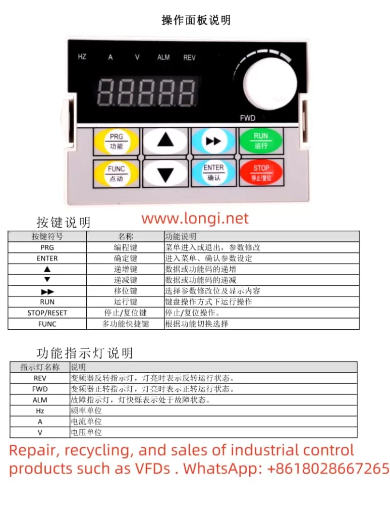
I. Operation Panel Function Introduction and Usage Instructions
The operation panel of the Yaskawa Inverter H1000 series serves as its control hub, enabling parameter setting, monitoring of operating status, and fault diagnosis. The primary buttons and functions on the operation panel include:
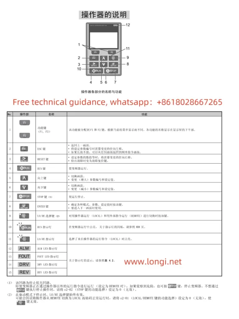
- ESC: Exits the current mode or cancels operations.
- RUN: Starts the inverter.
- STOP: Stops the inverter.
- ENTER: Confirms inputs or enters parameter settings.
- RESET: Resets faults.
- ALM: Displays fault or warning messages.
- DIGIT: Selects digits during parameter setting.
- OPRATOR: The operation panel display, which shows various information and parameters.
Parameter Initialization
Parameter initialization restores the inverter’s settings to the factory defaults. The steps are as follows:
- Enter Initialization Mode: Press the “ESC” button on the operation panel, then press “ENTER” to enter the parameter setting mode.
- Select Initialization Parameter: Use the “DIGIT” buttons to select parameter “A1-03” and press “ENTER”.
- Set Initialization Value: Set the value of “A1-03” to “2220” or “3330” for initialization of 2-wire or 3-wire sequential control, respectively.
- Confirm and Save: Press “ENTER” to confirm the setting, and the inverter will automatically restart and complete the initialization.
Setting and Resetting Passwords
To protect the inverter settings from unauthorized changes, passwords can be set. The steps are as follows:
- Enter Password Setting Mode: In the parameter setting mode, select “A1-04” and press “ENTER”.
- Enter Password: Use the “DIGIT” buttons to input a 4-digit password and press “ENTER” to confirm.
- Confirm Password: Enter the same password again to confirm the setting and press “ENTER”.
To reset the password, simply enter the correct password in the password input interface to unlock the parameter settings.
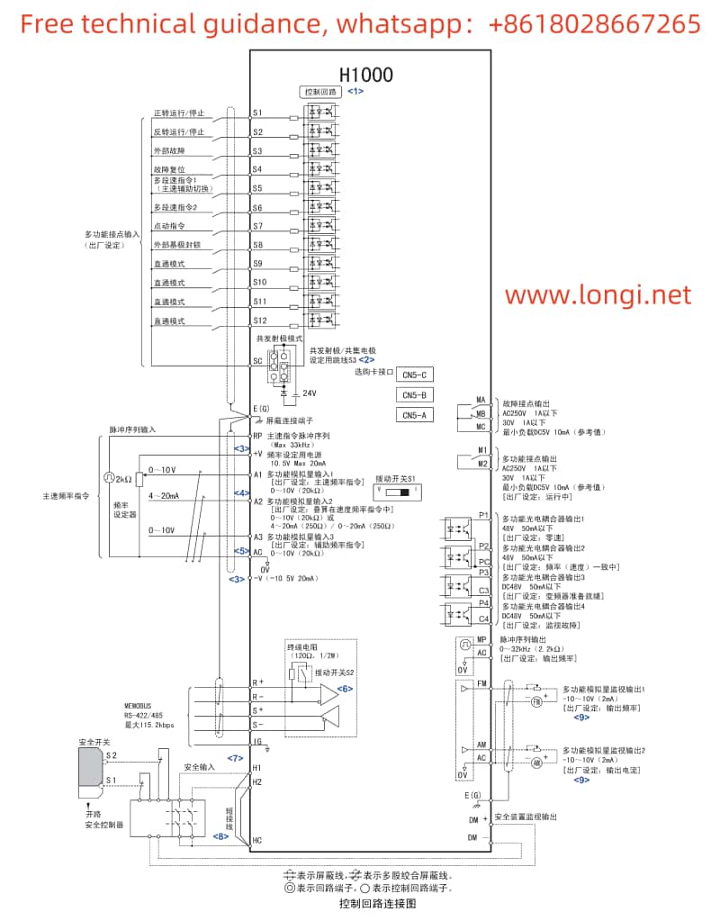
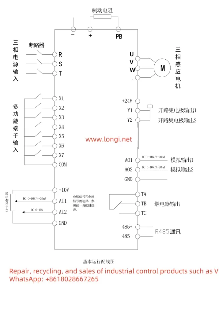
II. Terminal Start/Stop and External Potentiometer Speed Adjustment
To achieve terminal start/stop and external potentiometer speed adjustment, the corresponding control terminals need to be connected and parameters set accordingly.
Wiring Instructions
- Start/Stop Terminals: Typically, use terminals S1 (Run) and S2 (Stop). Closing (connecting) terminal S1 starts the inverter, while closing terminal S2 stops it.
- External Potentiometer: Use terminal A1 as the input terminal for the external potentiometer. Connect the potentiometer’s output to terminal A1 and adjust the potentiometer to change the frequency command.
Parameter Settings
- Run Command Selection: Set parameter “b1-01” to “10” to select the operation panel as the frequency command source.
- Multi-function Input Settings: Set parameter “H1-01” to “04” (Run command) and “H1-02” to “05” (Stop command), corresponding to the functions of terminals S1 and S2, respectively.
- Analog Input Gain and Offset: Adjust parameters “H3-03” (Gain) and “H3-04” (Offset) according to the output range of the external potentiometer to ensure that the frequency command changes proportionally with the potentiometer output.
III. Crane Control Wiring and Parameter Setup
In crane applications, special attention must be paid to safety control and precise speed regulation.
Wiring Instructions
- Main Circuit Wiring: Connect the inverter’s R/L1, S/L2, and T/L3 terminals to the crane motor according to its voltage and power requirements.
- Control Circuit Wiring: In addition to the basic start/stop terminals, emergency stop, limit switches, and other safety control terminals also need to be connected.
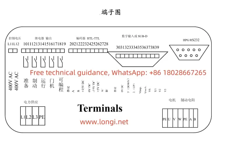
- PG (Encoder) Wiring: For cranes requiring precise speed control and positioning, connect the PG encoder and output its signals to the inverter’s PG option card.
Parameter Settings
- Control Mode Selection: Set parameter “A1-02” to the appropriate vector control mode (e.g., Vector Control with PG) to ensure precise speed and position control.
- PG Parameter Settings: Set parameters such as “F1-06” (PG Output Division Ratio) and “F1-12/F1-13” (PG Gear Ratio) according to the encoder specifications.
- Safety Function Settings: Enable the external emergency stop function and set the relevant parameter, such as “H2-01” (Multi-function Contact Output Selection), to output an emergency stop signal.
- Speed Search Function: For heavy-duty applications like cranes, it is recommended to enable the speed search function to improve stability and safety during startup. Set parameter “b3-01” to effective and adjust other related parameters as needed.
IV. Fault Code Meanings and Solutions
The Yaskawa Inverter H1000 series has comprehensive fault self-diagnosis functions. When a fault occurs, the operation panel will display the corresponding fault code. Below are the meanings of some common fault codes and their solutions:
- CPF00/CPF01: Control circuit fault. Possible causes include incorrect control circuit wiring or damaged circuit boards. The solution is to check the control circuit wiring and replace the circuit board if necessary.
- oH: Overheating of the heatsink. Possible causes are high ambient temperature, excessive load, or a faulty cooling fan. The solution is to improve ventilation, reduce the load, or replace the cooling fan.
- Uv: Undervoltage in the main circuit. Possible causes are low supply voltage or phase loss in the power supply. The solution is to check the supply voltage and wiring to ensure they are normal.
- oL1: Motor overload. Possible causes are excessive load or improper motor parameter settings. The solution is to reduce the load or reset the motor parameters.
When a fault occurs in the inverter, first check the fault code displayed on the operation panel to identify the cause and follow the corresponding solution. If the issue cannot be resolved, promptly contact a professional technician for repairs.
Through this operation guide, users can better understand and operate the Yaskawa Inverter H1000 series, ensuring its stable operation in various applications.