
The voltage amplitude of the six driving pulses outputted by the driving circuit meets the requirements. For example, measuring the amplitude of the positive excitation pulse voltage in the AC range is about 14V, and the amplitude of the negative cutoff voltage is about 7.5V (different models may vary). After the above inspection of the driving circuit, most maintenance personnel believe that the machine can be installed, but an extremely important inspection step – the inspection of the current (power) output ability of the driving circuit! Many VFDs that we believe have been repaired normally will still expose more hidden faults during operation, leading to a certain repair rate.
VFD operates normally under no-load or light load, but after carrying a certain load, it may experience motor vibration, output voltage phase deviation, frequency jump OC faults, etc.
Cause of malfunction: A. Insufficient output capacity of the power supply current (power) of the driving circuit; B、 The driving IC or the post amplifier of the driving IC is inefficient, and the output internal resistance increases, resulting in insufficient voltage or current amplitude of the driving pulse; C. IGBT is inefficient, with increased internal resistance and increased pressure drop in the conduction tube.
The proportion of failures caused by reason C is not high, and is limited by the conditions of the maintenance department, such as the inability to provide rated load testing for the frequency converter. But for the hidden faults caused by reasons A and B, we can use the method of increasing the load on the driver to expose them and then repair them, which can reduce the repair rate to the lowest level.
The normal opening of IGBT requires not only sufficient excitation circuit amplitude, such as+12V or above, but also sufficient driving current to ensure its reliable opening, or to ensure its conduction under a certain low internal resistance. The essence of the causes of faults A and B mentioned above is that due to the insufficient power output capability of the driving circuit, although the IGBT can be turned on, it cannot be in a good low conductivity internal resistance state, resulting in output phase deviation, severe motor vibration, and frequency jump OC faults.
Let’s conduct a more in-depth analysis of the control characteristics of IGBT and identify the root cause of the fault.
I. Control characteristics of IGBT:
The common perception is that IGBT devices are voltage-controlled devices, which require a certain level of excitation voltage for gate bias control, without the need to draw excitation current. In low-power circuits, only digital gate circuits can drive MOS-type insulated gate field effect transistors. As an IGBT, the input circuit happens to have the characteristics of a MOS-type insulated gate field effect transistor, and can therefore also be considered a voltage-controlled device. This perception is actually biased. Due to structural and process reasons, a junction capacitance called Cge is formed between the gate and emitter junctions of the IGBT tube, which controls the turn-on and turn-off of the IGBT tube. In fact, the charging and discharging control of Cge is responsible for the control of the turn-on and turn-off of the IGBT tube. The +15V excitation pulse voltage provides a charging current path for Cge, which turns on the IGBT; the -7.5V negative pulse voltage “forcibly pulls out the charged charge” on Cge, which plays a role in rapidly neutralizing the charged charge, and turns off the IGBT.
Assuming that the IGBT tube only controls the on-off switching of a DC circuit with a zero operating frequency, and after the Cge is fully charged at one time, there is almost no need for charging and discharging control, it is reasonable to describe the IGBT tube in this circuit as a voltage control device. However, the problem is that the IGBT tube in the output circuit of the frequency converter operates at a frequency of several kHz, and its gate bias voltage is also a pulse voltage with a frequency of several kHz! On the one hand, for such high-frequency signals, the capacitive impedance exhibited by Cge is relatively small, resulting in a large charging and discharging current. On the other hand, to make the IGBT turn on reliably and quickly (striving to make the tube have a small internal resistance), it is necessary to provide as large a driving current (charging current) as possible within the allowable operating range of the IGBT. For the control of turn-off, it is also the same. It is necessary to provide a low-resistance (ohmic) external discharge circuit to discharge the charge on the gate-emitter junction capacitor very quickly!
As we all know, capacitors are energy storage components that do not consume power themselves, and are called capacitive loads. However, just like the principle of power transmission and distribution lines, in addition to the power supply having to provide reactive current (reactive power) for capacitive components, which increases the power capacity of the power supply, the reactive current inevitably brings losses in line resistance (line loss)! The power loss of the drive circuit mainly concentrates on the gate resistance and the conduction internal resistance of the final amplifier tube. We often see that the output stage of the drive circuit, especially for high-power VFDs, is actually a power amplifier circuit, often consisting of medium-power or even high-power transistors, several watts of gate resistance, and other components, indicating that the drive circuit of IGBT consumes a certain amount of power and needs to output a certain current.
From the above analysis, it can be seen that the IGBT tube used in the VFD output circuit should be a current or power drive device, rather than a pure voltage control device
II. The last testing content before installation:
To minimize the rate of rework, after conducting comprehensive testing on the drive circuit in sections 3 and 4, do not miss the inspection of the drive circuit’s load-bearing capacity.
The method is as follows:
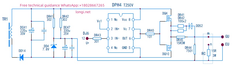
Measurement circuit for driving circuit with load capacity
The above diagram shows the driving circuit of the U-phase upper arm of DVP-1 22kW Delta VFD. The GU and EU in the figure are pulse signal output terminals, which are externally connected to the G and E poles of the IGBT. When repairing the drive board, it has been disconnected from the main circuit. The dashed box represents the external measurement circuit. After powering on the power supply/driver board, in conjunction with start and stop operations, a DC 250mA current range is connected in series at points m and n, and an external measuring resistor of 15 Ω 3W forms a circuit to detect the current output capability of each drive circuit. The starting state is measured, and five output current values are all around 150mA, with one output current only 40mA. The reason for the OC trip after installation and operation is precisely because the driving capability of this drive circuit is greatly insufficient! In the shutdown state, the measured current output capacity of each negative voltage power supply is about 50mA, and the negative voltage power supply capacity is normal.
Connecting RC in series plays a current limiting role, and the principle of its value is to select resistance and power values that are equal to the gate resistance (the parameter value of DR45 in the above figure) to make the detection effect obvious.
After testing the power output capability of the driving circuit, it can be determined that the driving circuit is completely normal. During the testing process of connecting the drive circuit to the main circuit, please first use a low-voltage 24V DC power supply to power the inverter circuit. After testing the drive circuit and inverter circuit to be normal, restore the normal power supply to the inverter circuit. If there is no low-voltage DC power supply at hand, at least two 45W light bulbs or 2A fuse tubes should be connected in series in the inverter power supply circuit. After the machine is tested normally, the original power supply of the inverter circuit should be connected!
The above power on detection of the driving circuit is carried out after disconnecting from the main circuit (IGBT). When the whole machine is connected, the input and input sides of the driving circuit must not be measured. Interference signals may be introduced due to human body induction and meter probes, causing IGBT to be triggered and conduct incorrectly, resulting in module explosion!
The insufficient output capability of the driving circuit is caused by two reasons:
A、 The power supply capacity is insufficient. Under no-load conditions, when we detect the output positive and negative voltages, they often reach the normal amplitude requirements. Even under load (such as after connecting to IGBT), although the instantaneous charging capacity of Cge is insufficient, due to the short charging time, we often cannot measure the low voltage drop of the power supply. Without resistive loads, this hidden fault can hardly be detected! The common fault in the circuit is the loss of capacitance of the filtering capacitor, as shown in DC41 in the figure above. Due to the drying up of the electrolyte inside the electrolytic capacitor during long-term operation, its capacity has decreased from a few hundred microfarads to several tens of microfarads, and even to a few microfarads. In addition, there may be inefficient rectifier tubes, such as an increase in forward resistance, which can also cause insufficient power output capacity;
B、 The internal output circuit of the driving IC is poor, or the internal resistance of the rear amplifiers DQ4 and DQ10 increases due to conduction. If there is no low drop in the power supply voltage after load testing, and the output voltage of T250 is detected to be low, it is a T250 defect. Otherwise, replace components such as DQ4 and DQ10. The phenomenon of increased resistance values such as DR40 and DR45 is relatively rare.
It should be noted that the insufficient positive excitation voltage only manifests as severe motor vibration, output voltage phase deviation, frequent OC faults, and other phenomena. Although it may cause overcurrent in the DC component of the motor winding, it poses a danger to the module structure that cannot be put into operation and the signal will burst. The loss of the negative cutoff voltage (caused by a fault in the negative pressure power supply circuit, which blocks the negative gate bias circuit) indicates that it is normal when powered on. When the start button is pressed, the IGBT inverter module will emit a “pop” sound and immediately burst into failure! Why is this?
III. Hazards of IGBT cut-off negative pressure circuit open circuit:
Except for the damage caused by sudden short circuit of the load during full speed operation, the harm of all faults such as overcurrent, overload, and undervoltage is far less than the harm of open circuit of gate bias circuit to IGBT. Speaking of this, maintenance personnel will deeply understand that they should not suffer too much from such losses.
During the maintenance process, the gate resistor DR45 was missed, and during the installation process, only the trigger plug of the upper arm IBGT1 was carelessly inserted, forgetting to connect the lower arm IGBT trigger terminal, resulting in the IGBT2 drive signal introduction terminal being vacant. After power on, the start signal is not activated, and there is no problem. Once the start signal is activated, there is no discussion, and the module is damaged. In my long-term maintenance work, I have developed a habit of stopping for a while before starting the operation after powering on, and observing whether the drive pulse output terminal is properly connected. After checking that each connection is intact, press the start button again. I often feel that this slight point is of great importance – the driving circuit and inverter output circuit are both in a normal state, and only one signal terminal of the driving pulse is missing, which will inevitably cause serious damage to the IGBT module and driving circuit again, resulting in all previous efforts being wasted!
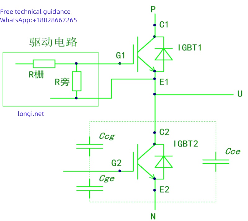
Just like bipolar devices – transistors, three wire components inevitably form three equivalent capacitors inside, while the Cge inside IGBTs is not parasitic, but formed by process and structure. Let’s not bother with Cce capacitors. The two capacitors, Ccg and Cge, can have a destructive effect on IGBT.
The above diagram shows the situation when the triggering terminal of the lower arm IGBT is open circuit. After power on, IGBT1 can maintain a reliable cut-off state by applying a negative cut-off voltage to the G and E poles due to the connection of the driving circuit. The reckless input of the frequency converter operation signal causes IGBT1 to be driven by a forward excitation pulse voltage and turn on. The C pole of IGBT2, the U terminal, immediately jumps to a DC high voltage of+530V. This jump voltage provides a charging return circuit for the Ccg and Cge capacitors. During the turning on period of IGBT1, IGBT2 is also driven by this charging current, and it is almost simultaneously turned on. The common connection of the two tubes forms a short circuit to the+530V power supply at the P and N terminals. With a loud bang, both tubes explode! If the signal terminal of the upper tube is empty and the lower tube is connected to the driving circuit, the conduction of the lower tube will also cause damage to both tubes for the same reason.
Assuming that there is a gate bypass resistor connected in parallel on the G and E poles of IGBT2 (such as the R side in the IGBT1 gate control circuit), it will form a bypass effect on the charging current mentioned above, and the possibility of the two transistors sharing the same circuit will be reduced. Assuming that during the conduction period of the upper tube, there is a cut-off negative pressure of about 7V between the G and E terminals of the lower tube, and the positive charging current is neutralized and absorbed by the gate negative bias, which is far from reaching the amplitude required to turn on the IGBT, then IGBT2 is safe. This is also why negative pressure is added to the control circuit of IGBT.
For frequency converters using IPM intelligent inverter modules, the driving power supply is often a single power supply without providing negative pressure. Is that the case?
From a design perspective, the shorter the lead of the IGBT drive signal, the better, in order to reduce the inductance effect of the lead; There should be a small resistance circuit between the E and E poles of the IGBT to fully bypass the interference signal current. The IPM module, driver circuit, and inverter main circuit are integrated inside the module, and the wiring between the driver circuit and IGBT is extremely short. According to data, even the gate resistance is omitted to reduce the wiring impedance. In the off state, IGBT ensures that the gate is in a low impedance grounded state, effectively preventing misleading conduction caused by interference signals, thus eliminating the need for negative power supply.