
The main circuit of the fault detection circuit is still composed of an operational amplifier. Usually, the operational amplifier is connected to the following types of circuits, completing three tasks of signal analog amplification, comparative output, and precision rectification.
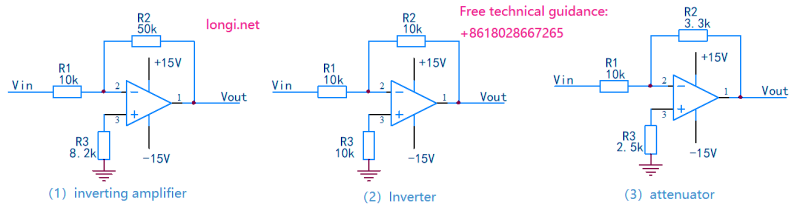
(A)、 Inverting amplifier circuit:
An operational amplifier has excellent characteristics such as high input impedance (without using signal source current), low impedance (with good load characteristics), amplification of differential mode signals (the difference between two input signals), suppression of common mode signals (with the same polarity and size of the two input terminals), and the ability to provide linear amplification for both AC and DC signals.
The figures (1), (2), and (3) in the circuit form are inverting amplifiers, where the output signal is in opposite phase to the input signal, also known as inverting amplifiers. The circuit has a dual amplification effect of voltage and current on the input voltage signal, but in small signal circuits, only the amplification and processing of the voltage signal are emphasized. The voltage amplification factor of a circuit depends on the ratio of R2 (feedback resistance) to R1 (input resistance). R3 is the bias resistor, and its value is the parallel value of R1 and R2. Due to the different values (ratios) of R2 and R1, three types of signal transmission functions can be completed, namely, forming three signal processing circuits: inverter amplifier, inverter, and attenuator. (1) The circuit is an inverting amplifier circuit with an amplification factor of 5; (2) The circuit is a inverter, which plays a reverse phase output role on the input signal and has no amplification factor, so it cannot be called an amplifier. Or input a 0-5V signal, then output a 0-5V inverted phase signal; (3) The circuit is an attenuator circuit. If a 0-10V signal is input, the output is 0-3. A 3V inverted signal is a proportional attenuator.
Figures (1), (2), and (3) have two characteristics of the circuit: 1. The input and output signals are reversed; 2. Whether it is an amplification, attenuation, or inverting circuit, the output signal maintains a proportional output relationship with the input signal, which can be broadly referred to as an inverting amplifier because the amplification factor of the inverter is 1, and the attenuator precisely utilizes the amplification effect of the circuit.
It is interesting that these three types of inverting amplifiers have applications in current and voltage detection circuits. Taking the current detection circuit as an example: This is because the current transformer connected in series to the three-phase output terminal has an amplifier built-in, and the output signal has reached a voltage amplitude of volts, while the input signal amplitude of the CPU must be within a voltage amplitude of 5V or less. Therefore, some reverse current signal processing circuits use reverse amplifiers with a certain amplification factor; Some use inverter circuits, which only perform inverter processing on the signal based on the polarity requirements of the CPU input voltage signal, without the need for further amplification; Some circuits are adapted to the signal amplitude range of the later stage circuit, and even use attenuator circuits to attenuate the voltage signal from the current transformer before sending it to the later stage circuit.
The power supply of the analog signal circuit in the detection circuit is generally powered by both positive and negative 15V dual power sources according to the requirements of amplifying AC signals. Based on the circuit form of the inverter amplifier and the circuit characteristics of the operational amplifier, we can find the corresponding detection method:
- According to the characteristics of the inverting amplifier, when a positive signal voltage is input, the input voltage must be negative below 0V, and vice versa, the output voltage must be positive above 0V, with 0V (ground) as the reference potential. To determine whether it is in a normal state based on the static circuit values of the circuit and input/output pins;
- Identify whether the circuit in this stage is an amplifier, inverter, or attenuator. Based on the ratio of input resistance to feedback resistance, the output voltage value can be roughly calculated to determine whether the circuit is in a normal state;
- According to the characteristic that the circuit has an amplification (or attenuation) effect on differential mode signals and a zero amplification effect on common mode signals, when short circuiting two input terminals, the output voltage should be close to the zero potential value; Alternatively, if there is a positive voltage (or negative voltage output) at the output terminal, but two input terminals are short circuited, the output voltage immediately drops (or rises) to around 0V. The circuit is good and can transmit signals normally.
- If the input voltage value can be artificially changed, the output voltage will inevitably change accordingly, which can be used to determine whether the amplifier is in a normal state.
[Fault Example 1]
After a certain frequency converter is powered on, an OC fault is reported, and the fault reset is invalid. The current detection circuit, as shown in the diagram (1), has an output voltage of+12V. The CPU reports an OC signal after power on due to a serious overcurrent signal input. Short circuit the 2 and 3 pins of the operational amplifier with metal tweezers, measure that there is no change in the output circuit of pin 1, and it is still+12V. It is judged that the operational amplifier is damaged. After replacement, the fault is eliminated.
[Fault Example 2]
A certain frequency converter outputs an undervoltage signal after being powered on, and detects the electrogram (2) circuit. The input voltage is -3V, but the output voltage is 0. 7V, indicating a malfunction of the amplifier in this stage. A 10k resistor was connected in series with an external DC 12V power supply, and the output voltage did not change when input to the reverse input terminal. It was determined that the amplifier in this stage was damaged, and the fault was resolved after replacement.
(B)、 In phase amplifier and voltage follower circuit:
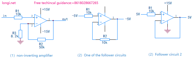
The circuit shown in Figure (1) is a typical circuit form of a in-phase amplifier, which is also one type of amplifier circuit. The input signal enters the same phase end of the amplifier, and the output signal is in the same phase as the input signal. The voltage amplification factor of the circuit is 1+R2/R1. It is also used for amplifying analog signals in fault signal detection circuits. When R2 is short circuited or R3 is open circuited, the output signal has the same phase and equal magnitude as the input signal, so (1) the circuit can further evolve into (2) and (3) circuits.
The above figures (2) and (3) show the voltage follower circuit. The output voltage completely tracks the amplitude and phase of the input circuit, so the voltage amplification factor is 1. Although there is no voltage amplification effect, it has a certain current output ability. The circuit plays a role in impedance transformation, improving the load capacity of the circuit and reducing the mutual influence of high impedance in the signal input circuit and low impedance in the output circuit. When used as a circuit follower, sometimes a single power supply is also used.
(1) The circuits (2) and (3) are also used in fault detection circuits for amplifying analog signals and processing reference voltage signals.
Based on the characteristics and functions of the circuit, the detection method can be obtained as follows:
- (1) The circuit is a in-phase amplifier circuit, and the output voltage amplitude and polarity are proportional to the input voltage. The voltage amplification factor of this stage is about 6 times. When the input voltage value is 1V, the output voltage is approximately 6V. It is possible to determine whether the circuit is in a normal state based on the calculation of input and output voltage values;
- (2) (3) The circuits are all voltage follower circuits, and the output voltage is completely tracked by the input voltage. The output voltage should be equal to the input voltage, which can be used to determine whether the circuit is in a normal state.
- By short circuiting two input terminals or manually changing the input voltage, the corresponding changes in the output voltage can be measured to determine whether the circuit is in a normal state.
[Fault Example 1]
A certain frequency converter experienced an OH fault when powered on. The reference voltage circuit of the temperature detection circuit, as shown in Figure (2), has an output voltage of 1V. This machine is a voltage comparator circuit, and its input voltage is measured to be 5V. Under normal conditions, the output voltage should also be 5V. After cutting off the output load circuit, the output voltage remains at 1. 2V, it was determined that the amplifier in this stage was damaged, and the fault was resolved after replacement.
(C) Precision positive and negative half wave rectifier and full wave rectifier circuits:
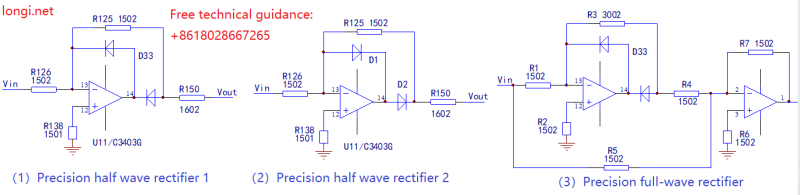
The AC voltage signal from the current transformer needs to be rectified into DC voltage through subsequent half wave or full wave rectification circuits, and then sent to the CPU for current display and control. Precision half wave or full wave rectification circuits are also used for processing and amplifying analog signals. Ordinary rectification circuits use diodes as rectification devices, but diode rectification has drawbacks such as nonlinear distortion and dead zone voltage. Especially when used for small signal rectification, it will cause output signal distortion and output errors. By utilizing the amplification effect and deep negative feedback effect of the operational amplifier, a diode is added to the amplification circuit. By utilizing the unidirectional conductivity characteristics of the diode, different depths of negative feedback are introduced to the input positive and negative half wave signals. The input μ V level signal can be rectified in a dense manner, and the circuit itself also has a voltage following or amplification effect.
The above figure (2) shows a precision negative half wave rectification circuit. The circuit will perform precision rectification on the input negative half wave signal and output it in reverse phase. For the positive half wave input signal, the connection of D1 introduces deep negative feedback to the amplifier; At the beginning of the negative half wave input signal, due to the signal input amplitude being smaller than D1 and D2, both are in the cut-off state, and the circuit is in an open-loop amplification state. A small signal input will cause the output pin voltage to be greater than -0. 7V, D1 conduction, D2 reverse bias cutoff; The series connection of D2 and R125 introduces moderate negative feedback (the resistance of R125 can determine whether the current circuit is a rectifier or a rectifier amplifier, and the current circuit is a precision rectifier with no amplification effect), which is equivalent to an inverter amplifier, and the output is inversely correlated with the input signal.
The difference between the circuit in Figure (1) and Figure (2) is that the polarity of the two diodes in the circuit is opposite, making it a precise rectification circuit for the input positive half wave signal. The principle of rectification is the same.
By adding a half wave rectifier circuit and an inverse summation circuit, as shown in Figure (3), the positive and negative half waves are input and output in reverse to obtain a full wave output voltage waveform, forming a high-precision full wave rectifier circuit.
In fault detection circuits, rectifier circuits are often used to sample the three-phase output current signal, which is rectified and amplified as an analog voltage signal (current detection signal) input into the subsequent fault signal processing circuit and CPU circuit, used for overload alarm and sampling processing of operating current.
The input of the circuit is an AC voltage signal, while the output is a DC voltage signal. Most circuits are rectifiers, and some circuits are rectifier amplifiers.
Detection method:
- Rectifier circuit: The input side is AC voltage, and the output side is DC voltage. The two measured values are relatively close.
- Rectifier amplifier, with AC voltage on the input side and DC voltage on the output side. The output DC voltage value is higher than the input AC voltage value.
- By short circuiting two input terminals or manually changing the input voltage, the corresponding changes in the output voltage can be measured to determine whether the circuit is in a normal state.
[Fault Example 1]
A certain frequency converter experienced an OC fault when powered on. The output voltage of the current detection circuit as shown in Figure (2) was 13V. After unplugging the lead terminal of the current transformer, the amplifier in that stage still had 13V. It was determined that the rectifier circuit was damaged and the fault was resolved after replacement.
(C) Circuit for voltage comparator, step voltage comparator, and window voltage comparator:
The above-mentioned circuits are all used for amplifying and rectifying analog signals, and their output signals still have analog signals, which can be called analog signal (amplification) processing circuits. However, in the following voltage comparison and other circuits, the output is a switch signal. The circuit has left the scope of analog amplification and seems to have entered the field of “digital circuits”, using analog circuits as digital circuits for application.
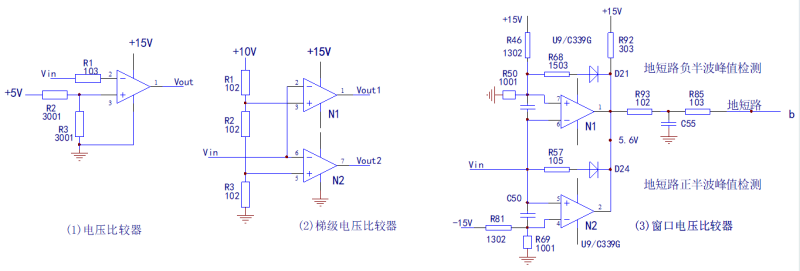
The function of a voltage comparator is to compare the magnitude of two input voltage signals. In Figure (1) of the circuit, the voltage at the same phase input end of the amplifier is the voltage divider value 2 of R2 and R3 resistors to+5V. 5V, known as the reference voltage value, compares the input signal with this reference value. When it is higher than this value, it outputs a 0V low-level signal. When it is lower than the low value, it outputs a+15V high-level signal. Circuit, also known as a single value comparator, the output state of the circuit depends on a value (a point) of the input signal voltage -2. 5V.
If the two-stage voltage comparator is connected to the circuit shown in Figure (2), it becomes a stepped voltage comparator. The circuit has one input signal and two output signals. The N1 and N2 voltage comparators input the same signal voltage, but the reference voltage values at the same phase input terminals of the two-stage circuit are different. The N1 reference voltage is 6. The reference voltage value for 6V and N2 is 3. 3V. When the input signal gradually increases from 0V to 3. When the voltage is above 3V, the output state of N2 first changes to low level; N2 has an input signal value greater than 6. At 6V, there is only a low-level signal output. When the circuit in Figure (2) is used for voltage detection in the DC circuit, when the regenerative energy generated by the load motor is fed back to the DC circuit, causing the DC circuit voltage to rise to a certain value, N2 first outputs a braking action signal, connects the braking resistor to the DC circuit, and consumes the voltage increment; If the voltage continues to rise, N1 will output an OU overvoltage signal, and the frequency converter will shut down for protection.
If the two-stage voltage comparator is connected to the circuit shown in Figure (3), it constitutes a window voltage comparator circuit. Compared to single-stage voltage comparator circuits, window voltage comparators can be referred to as dual value comparators. The circuit has two benchmark comparison values and outputs one signal. When the input signal is ≥ reference voltage 1 ≤ reference voltage 2, the circuit output state transitions. Within a range of the intermediate value of the input signal, the output state remains unchanged. The circuit in Figure (3) is a ground fault signal processing circuit. The in-phase end of the N1 amplifier is the voltage divider of R46 and R50 to+15V, while the reverse end of the N2 amplifier is the voltage divider of R81 and R69 to -15V. The input three-phase current sampling signal enters the reverse input terminal of N1 and the in-phase input terminal of N2, and is compared with the positive and negative partial voltage values, respectively. Whether it is the positive half wave or negative half wave of the input signal, as long as it is greater than the two reference values, a ground short circuit signal will be reported.
The voltage comparator uses digital circuits, which can flexibly set the reference voltage based on the signal amplitude, making it more convenient than using digital circuits. In addition, the circuit in Figure (3) adopts an operational amplifier circuit with an open collector output, which can achieve parallel output at the output end, making the circuit more concise. If a regular amplifier is used, the output signal also needs to be isolated by two diodes and connected together in parallel.
Three types of voltage comparator circuits are commonly used to convert analog signals of detected current or voltage into switch signal – fault signal output, for implementing control actions and shutdown protection.
Detection method:
- The amplifier output has only two level states, low level, close to the ground level of the power supply or negative power supply value; High level, close to positive power supply value;
- If the voltage value of the inverting input terminal is lower than that of the in-phase input terminal, the output is low level; otherwise, the output is high level.
- By short circuiting two input terminals or manually changing the input voltage, the corresponding changes in the high and low levels of the output terminals can be measured to determine whether the circuit is in a normal state.
(E) Hysteresis comparator circuit:
It is also one of the voltage comparator circuits. The circuit in Figure (3) of the voltage comparator, also known as the hysteresis voltage comparator circuit. The voltage comparator circuit can be upgraded to a hysteresis comparator circuit by introducing an additional positive feedback circuit. Hysteresis comparator circuits are referred to as voltage comparator circuits with hysteresis characteristics. If ordinary voltage comparison is regarded as “voltage point comparison”, hysteresis comparator can be regarded as a comparator circuit for “voltage range comparison”. Usually, we hope that the output state of the circuit is stable enough, and comparing the voltage at a “point” can cause instability in the output state due to frequent output. Improving the “point” comparison of the input circuit to “segment” comparison can effectively solve this problem – within a “segment value” of input voltage variation, the output state remains unchanged. Figure (2) shows a positive feedback branch composed of R4 and D1, which converts the “point” comparison characteristic of the circuit into a “segment” comparison characteristic.
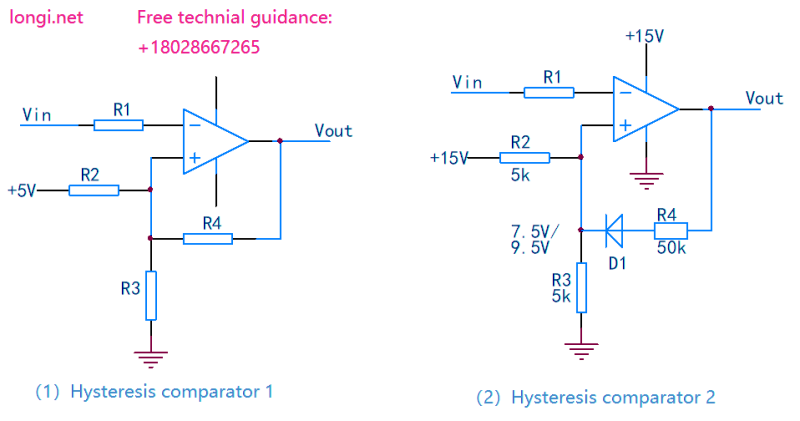
The control principle is briefly described as follows:
Assuming that the circuit in Figure (2) is used for processing the braking action signal, the input signal is the voltage sampling signal of the DC circuit. When the voltage of the DC circuit rises abnormally due to the energy feedback from the load motor, reaching 680V, the input voltage value of Vin reaches 9. When the voltage is above 5V and higher than the reference voltage at the reverse end of the amplifier, the amplifier outputs a low-level signal, and the subsequent braking circuit acts, connecting the braking resistor to the DC circuit to consume the voltage increment; Due to the consumption effect of the braking resistor, the input voltage value of Vin quickly drops to 9. Below 5V, but the braking signal is still being output, and it does not mean that the DC circuit voltage slightly drops, causing the braking signal to disappear. This indicates the role of the hysteresis comparator. The braking circuit continues to operate until the DC circuit voltage returns to below 620V, and the sampled input voltage is below 7. The braking circuit only stops working at 5V.
When the circuit is static, the voltage at the same phase end of the amplifier (7.5V) is higher than the voltage at the opposite phase end, and the output voltage is a high-level voltage of nearly 15V. R4 and D1 are introduced into the same phase end circuit, artificially raising the same phase end voltage to 9. 5V. When the input voltage is above 9. At 5V, the circuit output state reverses and the output end becomes low level. D1 reverse bias cutoff, feedback loop interruption, and reference voltage at the same phase end restored to 7. 5 V partial voltage value. In this way, when the input sampling voltage is below 7. At 5 V, the brake signal stops outputting.
Hysteresis comparator circuits are commonly used for voltage detection in DC circuits, outputting braking signals and overvoltage/undervoltage fault signals.
The detection method is the same as the voltage comparator, omitted.