
If you frequently repair a certain brand or several brands of inverters, you should have the terminal diagram of the connection cable between the CPU motherboard and the power/driver board. With it, the maintenance efficiency will be greatly improved. I spent a lot of effort to survey and map the terminal diagrams of the CPU motherboards of three inverters. I dare not keep it secret, so I share it here with you.
The above figure shows the function/destination (50 lines) of the TECO 7300PA inverter mainboard wiring terminal 7CN. The inverter of this model has excellent versatility in CPU mainboards, ranging from 22kW to 300kW, and can be interchanged. You only need to adjust the parameter “inverter capacity”. That is to say, this brand of inverter, due to different power levels, except for the power supply/driver board, actually uses the same CPU mainboard, so this terminal diagram can be used for “all sizes” during maintenance.
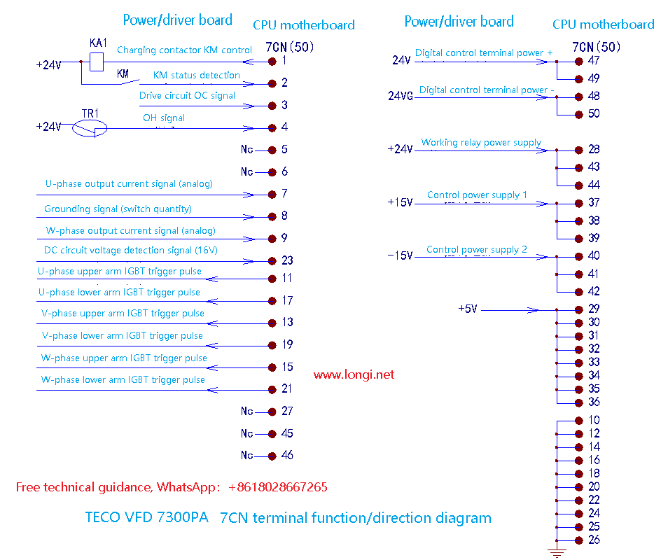
Using the terminal diagram:
1. Check the input and output control signals. Most of them are switch signals, and the high and low level values are very obvious. For example, the detection signal terminals 2 and 4 of the charging contactor and temperature sensor have a terminal voltage of 24V when normal and 0V when abnormal. The static and dynamic (start/stop) voltage values of the six-way pulse signal terminals are obvious; although the output current detection signal is an analog quantity, it should be 0V when static and unloaded. Generally, it is about 2V when fully loaded.
2. You can “play tricks” on the terminals. For example, if the module overheats, you can try to short-circuit terminal 4 and pin 28. If the fault disappears, it means that the external temperature relay (sensor) at terminal 2 is faulty. If the fault still exists, it means that the fault is in the subsequent temperature signal processing circuit.
If you connect a potentiometer between terminals 10 and 29 and connect its center arm to the output current detection terminal (terminal 7 or 9), you can simulate a load test to check whether the subsequent current detection circuit is normal.
If an analog signal only deviates from the normal value (and still works), and falsely reports an “overvoltage” fault under normal power supply, you can use parallel and series resistance methods at terminals 23 to make its voltage value fall back to the normal detection value for emergency repair.
[ Failure Example 1 ] :
A 300kW7300PA inverter has an output frequency display on the operation display panel, but there is no three-phase voltage output on the U, V, and W terminals. After disconnecting the power supply of the inverter circuit, the six pulse signals of the 11, 13, 15, 17, 19, and 21 pins of the 7CN terminal were measured and all were normal. It was determined that the fault was in the pulse pre-stage signal circuit of the power supply/driver board. From these six terminals, it was quickly found that U12 (MC14069) was defective. After replacement, the fault was eliminated.
[ Failure Example 2 ] :
A 300kW7300PA inverter reported a “DC circuit undervoltage” fault after power-on and could not start running. The DC circuit voltage detection signal of terminal 23 of the wiring terminal 7CN was normal. After power-on, the measurement of terminal 2 was always low level, indicating that the auxiliary contact of the charging contactor was not closed. The CPU detected that the charging contactor was not closed, so it reported an undervoltage fault.
Try to short-circuit terminal 2 and terminal 28, and it runs normally.
Check from terminal 2 to the power supply/driver board and find out that the normally open contact of relay KA1 is connected in series in the 2-terminal circuit. The contact of KA1 is in poor contact. Replace KA1 and the fault is eliminated.
[ Failure Example 3 ] :
A 7300PA37kW inverter reported an OC fault as soon as it was powered on. The power supply of the current detection circuit was detected from the terminals. The -15V of terminals 40, 41, and 42 was 0V. Due to the abnormal power supply, the output of the current detection circuit was offset and an OC fault was reported. The -15V rectifier diode of the switching power supply was checked and found to be open. The fault was eliminated after replacement.
In the above three faults, with the guidance of the 7CN terminal diagram, the faults were found quickly and accurately in a very short time and the faults were eliminated efficiently.
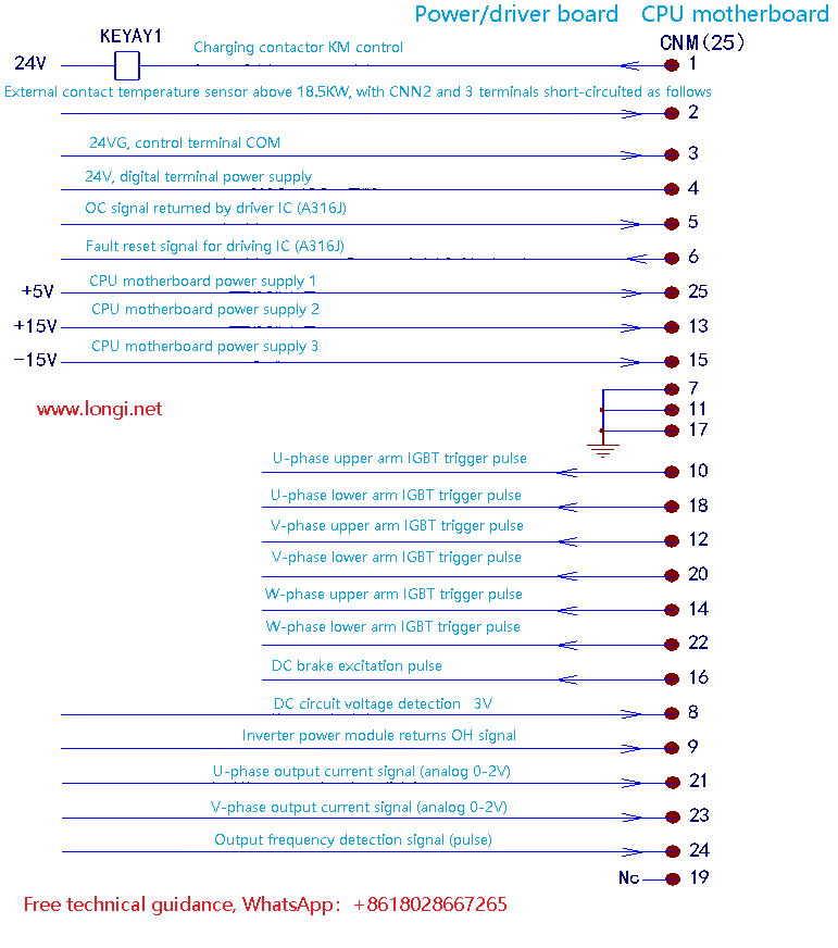
The above picture is the Alpha inverter CPU motherboard CNM wiring terminal diagram, a total of 24 lines. Although the CPU motherboard of this model cannot be replaced – the overload protection and other parameters are fixed and the relevant parameter values cannot be modified; the CPU motherboard circuits are also different. I have seen two motherboard circuits, but the CNM terminals are the same. Therefore, the CNM terminal function/destination diagram is still very valuable as a “guide” for maintenance.
[ Failure Example 1 ] :
An Alpha 2000 15kW inverter tripped an undervoltage fault as soon as it was started, and no charging contactor closure sound was heard when it was powered on. The CNM terminal 1 was tested and was always at a high level of 24V, indicating that the charging relay control circuit was faulty. From terminal 1 to the CPU mainboard, it was determined that the circuit inside the CPU control pin was damaged.
Emergency repair: Short-circuit terminal 1 and terminal 7. After the switching power supply starts to oscillate, force the charging relay to be energized and closed to eliminate the fault.
[ Failure Example 2 ] :
An Alpha 2000 18.5kW inverter, with a load rate of less than 50%, but the on-site power supply fluctuates greatly, sometimes as low as 320V. The inverter tripped an undervoltage fault, and the dealer and the user required measures to make the inverter run. Cut the cable of CNM terminal 8, connect a 4.7kΩ semi-variable resistor between terminals 25 and 7 , connect the center arm to terminal 8, and adjust it to a fixed voltage of 3V.
The inverter no longer trips the undervoltage fault and operates normally. (This emergency measure must be used with caution in specific applications!)
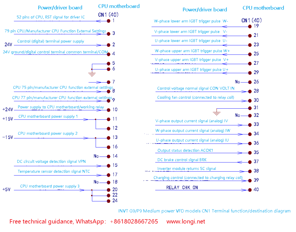
There is a trick to speed up the inspection, which is to make a diagram of the motherboard wiring terminals. Clearly mark the terminal serial number and the source and destination of the terminal signal. It would be even better if the dynamic and static voltage values of each terminal could be marked. Fortunately, there are many switching signals, which are easier to detect and judge. Analog signals also have obvious differences in dynamic and static, which are easier to detect.
The figure above is the function/destination diagram of the CN1 terminal. For terminals 4, 7, 8, and 9, the terminals are set by the manufacturer. Except for replacing the CPU motherboard, you can check the short-circuited state of the terminals. For maintenance, it is useless, so don’t worry about it. 24V, +15, -15V, +15V, and +5V power supplies are the 5 power supplies commonly used by the CPU motherboard. Some inverters have two 24V power supplies, one for the control relay coil and the other for the control sub-power supply. The power supply introduction in the terminal occupies most of the terminals, six inverter pulses, and some have one DC braking pulse, which occupies part of the terminals. The others are various input/output, switch quantity/analog quantity signal terminals. What we need to pay attention to and frequently test is this third type of terminal. When checking a certain circuit, you can also artificially change the voltage state of this type of terminal to see if the corresponding circuit reacts. By observing or measuring the normal or abnormal reaction of the corresponding circuit, you can clearly judge whether the circuit is good or bad.
[ Failure Example 1 ] :
An INVT G9/P9 5.5kW inverter has an unbalanced output three-phase voltage. After disconnecting the inverter power supply, the start signal is input and the six pulse signal terminals 19, 21, 23, 25, 27 and 29 of CN1 are detected. It is found that the voltage at pin 21 is fixed and there is no change in dynamic or static state. It is judged that the fault is in the pulse pre-stage circuit or the PWM pulse output pin of the CPU.
Check the inverter pulse pre-stage circuit U4 (LS07), the six-way inverter pulse at the input end is normal, and there is no signal voltage output at the output pin 8. Replace U4 and the fault is eliminated.
[ Failure Example 2 ] :
An INVT G9/P9 5.5kW inverter reported an undervoltage fault during operation. The CN1 terminal 39 pin was detected to be low level, indicating that the CPU has output a charging relay closing signal. The charging relay was checked and found to have been replaced. The coil solder joints were poorly soldered. After re-welding, the fault was eliminated.