
In the realm of industrial machinery, frequency converters play a crucial role in controlling motor speed and efficiency. However, when dealing with high inertia loads, such as in mining elevators or high-speed lifts, the motor can transition from an “electric” state to a “dynamic” state, temporarily becoming a generator. This phenomenon results in regenerative energy flowing back into the system, which can cause voltage spikes and potentially damage the frequency converter’s components. To mitigate these issues, brake units and braking resistors are often integrated into the system. This article delves into the workings of a brake unit, its circuit diagram, and troubleshooting tips.
The Role of Brake Units
When a motor decelerates, brakes, or lowers a heavy load, the mechanical system’s potential energy can cause the motor’s actual speed to exceed the frequency converter’s set speed. This leads to a capacitive current in the motor windings, which generates excitation electromotive force, causing the motor to self-excite and generate electricity. This electrical energy is then fed back into the power grid. However, this regenerative energy can cause the voltage in the frequency converter’s DC circuit to rise sharply, potentially damaging the energy storage capacitors and inverter module.
To prevent this, brake units and braking resistors are used. A brake unit is essentially an electronic switch (IGBT module) that, when activated, connects the braking resistor to the DC circuit. This rapidly dissipates the motor’s regenerative energy as heat, keeping the DC circuit voltage within safe limits.
Circuit Analysis
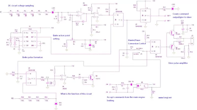
The brake unit’s control circuit typically includes a DC voltage detection circuit that triggers the electronic switch when the DC circuit voltage exceeds a certain threshold (e.g., 660V). Once the voltage drops below a lower threshold (e.g., 620V), the switch turns off.
In more advanced systems, the brake unit’s performance is optimized through pulse braking. Here, a voltage/frequency or voltage/pulse width conversion circuit controls the IGBT module’s on/off state. When the DC circuit voltage is high, the braking unit operates at a higher frequency or longer conduction cycle, and vice versa.
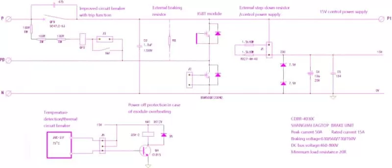
The CDBR-4030C Brake Unit
The CDBR-4030C brake unit, while not the most optimized in terms of structure and performance, is still effective in practice. It uses a dual-tube IGBT module, although only one tube is utilized, making it somewhat inefficient. The protective circuit combines electronic and mechanical trip circuits, with the QF0 air circuit breaker modified to trip when the module overheats.
Common Faults and Repairs
Faults in the brake unit often occur in the control power supply circuit, such as an open circuit in the step-down resistor or a breakdown in the voltage regulator. Additionally, moisture can reduce the insulation in the frequency converter’s DC circuit, leading to high voltage discharge and circuit board damage.
The brake unit’s control circuit typically includes an LM393 operational amplifier, a CD4081BE four-input AND gate, and a 7555 (NE555) timer circuit. Troubleshooting involves checking these components and their connections.
One unique feature of the circuit is the hysteresis voltage comparator, which prevents frequent output fluctuations by providing a certain hysteresis voltage. If the braking unit fails to operate correctly, it could be due to issues in this comparator or the voltage comparator connection.
Protective Measures
The circuit also includes protective measures to prevent damage to the IGBT module. For instance, if the module temperature rises to 75°C, a temperature relay triggers a trip, cutting off the brake unit’s power supply. Additionally, the circuit design ensures that if the braking resistor remains connected or the IGBT module fails, the system will shut down to prevent further damage.
Conclusion
Understanding the workings of a brake unit and its circuit diagram is essential for effective troubleshooting and repair. By analyzing the control principle and common faults, technicians can quickly diagnose and resolve issues, ensuring the smooth operation of frequency converters in industrial applications. With proper maintenance and repairs, brake units can provide reliable protection against voltage spikes and regenerative energy, prolonging the lifespan of frequency converters and their components.