Introduction
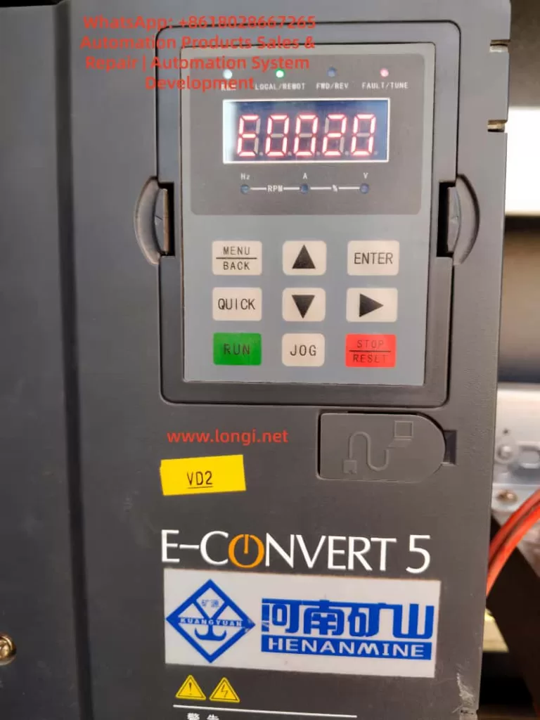
In the field of modern industrial automation, inverters, as the core equipment for motor control, play a crucial role in ensuring production safety and improving equipment utilization. The E-CONVERT 5 series inverter launched by WISCO South (Wuhan) Automation Co., Ltd. has gained widespread market recognition for its high performance, high reliability, and rich functionality. However, during actual operation, the E0020 contactor fault, as a relatively common type of fault, poses a threat to the normal operation of the equipment. This article will provide a detailed analysis of the meaning, causes, diagnostic methods, and handling measures of the E0020 fault, aiming to assist technicians in quickly locating problems and restoring normal equipment operation.
brp_del_th:null;
brp_del_sen:null;
delta:null;
module: photo;hw-remosaic: false;touch: (-1.0, -1.0);sceneMode: 8;cct_value: 0;AI_Scene: (-1, -1);aec_lux: 0.0;aec_lux_index: 0;HdrStatus: auto;albedo: ;confidence: ;motionLevel: -1;weatherinfo: null;temperature: 28;
I. Overview of E0020 Fault
1.1 Fault Definition
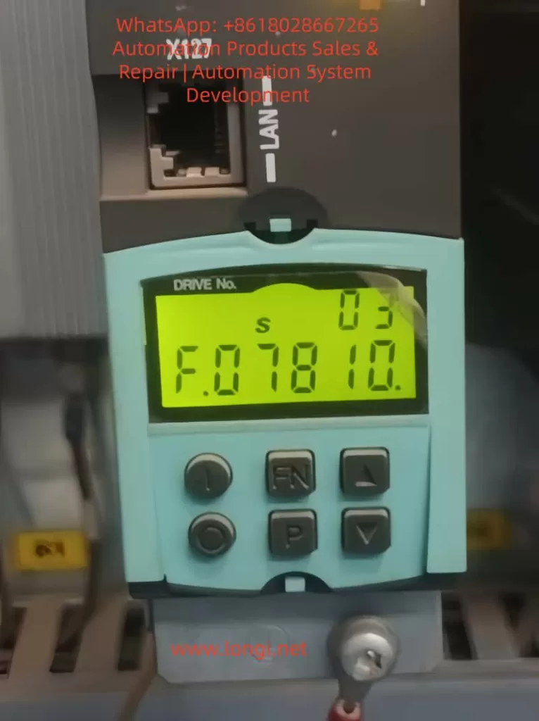
The E0020 fault code in the WISCO South E-CONVERT 5 series inverter represents a contactor fault. When the inverter detects that the contactor fails to engage normally or exhibits abnormalities during startup or operation, it triggers this fault code, causing the inverter to stop working and display corresponding fault information.
1.2 Fault Impact
As a key connecting component between the inverter and the motor, the contactor’s normal operation is vital for the motor’s startup, operation, and shutdown. Once a contactor fault occurs, it will directly affect motor control, potentially leading to production line shutdowns, equipment damage, or even safety accidents.
II. Causes of E0020 Fault
2.1 Contactor Faults
- Contact Wear or Adhesion: After prolonged operation, the contacts of the contactor may become worn or adhered due to arc erosion, resulting in poor contact or an inability to disconnect.
- Coil Faults: The contactor coil may be damaged due to voltage fluctuations, overheating, etc., leading to an inability to engage or maintain engagement.
- Mechanical Faults: The internal mechanical structure of the contactor (such as springs, armatures, etc.) may experience wear, deformation, etc., causing sluggish action or seizure.
2.2 Control Circuit Issues
- Abnormal Control Signals: The control signals output by the inverter may prevent the contactor from engaging normally due to line faults, interference, etc.
- Incorrect Parameter Settings: Parameters within the inverter related to contactor control (such as engagement time, release time, etc.) may be set improperly, causing abnormal contactor action.
- Program Errors: The inverter’s control program may contain logical errors or bugs, leading to incorrect or unsent contactor control commands.
2.3 Power Supply Problems
- Unstable Power Supply Voltage: Excessive fluctuations in the power supply voltage may result in insufficient or excessive voltage at the contactor coil, affecting its normal operation.
- Power Supply Phase Loss: The absence of any phase in a three-phase power supply will prevent the contactor from engaging or maintaining engagement.
2.4 Environmental Factors
- High Temperature: Excessively high operating temperatures in the inverter’s environment may accelerate the aging of internal components in the contactor, degrading performance.
- High Humidity: High humidity environments may cause condensation, short circuits, etc., inside the contactor.
- Dust Pollution: Dust entering the contactor may affect the quality of contact between the contacts, leading to poor contact.
III. Diagnostic Methods for E0020 Fault
3.1 Visual Inspection
- Observe the appearance of the contactor to check for damage, deformation, burning, etc.
- Inspect the connecting wires to confirm they are not loose, detached, or damaged.
3.2 Electrical Measurement
- Use a multimeter to measure the voltage across the contactor coil to confirm whether the voltage is normal and stable.
- In a de-energized state, use a multimeter to measure the resistance value of the contactor contacts to confirm whether the contacts are in good contact.
3.3 Control Signal Inspection
- Inspect the control signal lines to confirm they are intact and free from short circuits or open circuits.
- Use an oscilloscope to observe the waveform of the control signal to confirm whether the signal is stable and meets the inverter’s requirements.
3.4 Parameter and Program Inspection
- Verify the parameter settings within the inverter related to contactor control to confirm they are correct and error-free.
- If possible, debug and inspect the inverter’s control program to confirm the correctness of the program logic.
3.5 Environmental Inspection
- Confirm whether the inverter’s operating environment meets requirements, including temperature, humidity, dust, etc.
- Clean the inverter and contactor to remove dust and dirt.
IV. Handling Measures for E0020 Fault
4.1 Replacing the Contactor
- Confirming the Fault: After completing the above diagnostic steps, if it is confirmed that the contactor itself has a fault and cannot be repaired, promptly replace it with a contactor of the same model and specifications.
- Replacement Steps:
- Disconnect the power supply to the inverter and confirm there is no electricity.
- Remove the faulty contactor and record its wiring method.
- Install the new contactor and connect the wires according to the original wiring method.
- Restore the power supply and test whether the contactor operates normally.
4.2 Repairing the Control Circuit
- Repairing Line Faults: If short circuits or open circuits are found in the control signal lines, promptly repair or replace the lines.
- Adjusting Parameter Settings: Adjust the parameter settings related to contactor control within the inverter according to the inverter’s manual to ensure the parameters are reasonable and meet actual needs.
- Repairing Program Errors: If logical errors or bugs are found in the control program, promptly contact the manufacturer or professional personnel for repair.
4.3 Improving Power Supply Quality
- Stabilizing Power Supply Voltage: Install voltage stabilizers, UPS devices, etc., to stabilize the power supply voltage and reduce the impact of voltage fluctuations on the contactor.
- Checking for Power Supply Phase Loss: Use a phase sequence meter to check whether the three-phase power supply is missing any phase and promptly address the power supply phase loss issue.
4.4 Optimizing the Operating Environment
- Controlling Temperature: Install air conditioners, ventilation equipment, etc., to control the operating temperature of the inverter’s environment within a reasonable range.
- Reducing Humidity: Use dehumidifiers, desiccants, etc., to reduce the humidity of the operating environment and prevent condensation and short circuits.
- Reducing Dust: Regularly clean the inverter and contactor to reduce the impact of dust pollution on the equipment.
V. Preventive Measures and Routine Maintenance
5.1 Regular Inspection and Maintenance
- Developing a Maintenance Plan: Formulate a regular maintenance plan based on the equipment’s usage and the manufacturer’s recommendations, including contactor inspection, line tightening, parameter verification, etc.
- Executing Maintenance Tasks: Regularly perform maintenance tasks according to the maintenance plan to ensure the equipment is in good condition.
5.2 Training and Operating Specifications
- Training Technicians: Provide professional training to equipment operators to improve their understanding and handling ability of inverter and contactor faults.
- Developing Operating Specifications: Formulate detailed equipment operating specifications and maintenance procedures to ensure operators follow the specifications for operation and maintenance.
5.3 Spare Parts Management
- Stocking Spare Parts: Stock necessary spare parts (such as contactors, coils, etc.) based on the equipment’s usage and historical fault records to enable prompt replacement in case of faults.
- Managing Spare Parts: Establish a spare parts management system to regularly inspect and update spare parts, ensuring they are of reliable quality and sufficient quantity.
VI. Conclusion
The E0020 contactor fault is a relatively common type of fault during the operation of the WISCO South E-CONVERT 5 series inverter. By thoroughly analyzing the fault causes, adopting scientific diagnostic methods, and implementing effective handling measures, normal equipment operation can be quickly restored, and the impact of faults on production can be reduced. Meanwhile, by formulating preventive measures and strengthening routine maintenance management, the reliability and stability of the equipment can be further improved, creating greater economic and social benefits for enterprises.