In industrial automation, the inverter plays a crucial role in motor speed regulation and energy saving. Its stability directly affects the efficiency and reliability of the entire system. This article focuses on the SC1 fault code commonly seen in the Panasonic VF0 series inverter, analyzing its meaning, root causes, and practical troubleshooting steps.

1. What Does SC1 Fault Indicate?
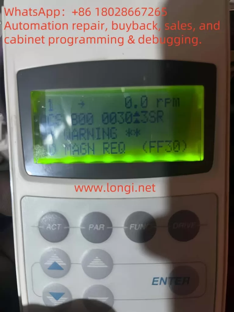
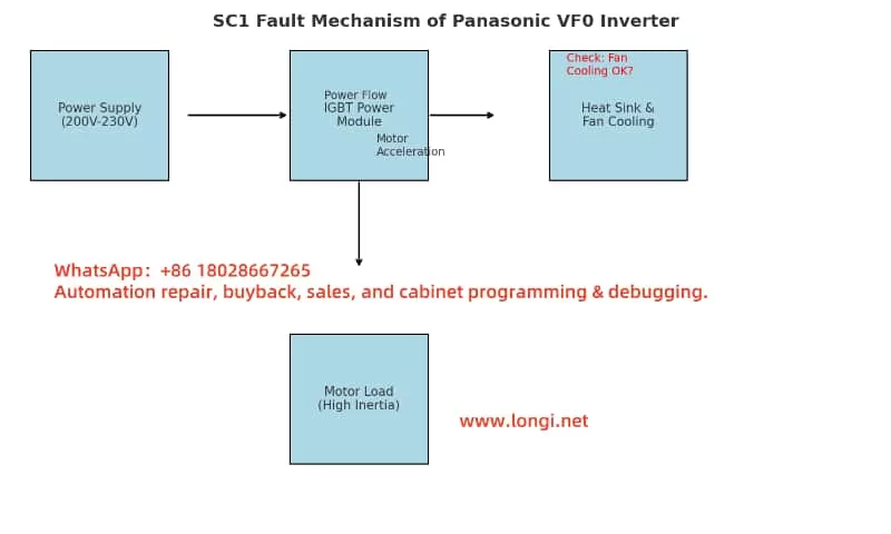
According to the Panasonic VF0C Inverter Manual, the SC1 code signifies an overcurrent or abnormal heat generation at the heatsink during acceleration. It is a protective mechanism to prevent IGBT modules or internal circuits from damage caused by excessive current or temperature spikes.
- SC1: Overcurrent or overheating during motor acceleration phase
- Main protection target: IGBT modules, bus capacitors, cooling fans
- Trigger timing: During the acceleration ramp-up of the motor
2. Common Causes of SC1 Fault
SC1 faults can arise due to issues in power electronics, load mechanics, thermal conditions, or control parameters. The most frequent causes include:
a) Output Short Circuit or Ground Fault
Faulty motor cables or incorrect wiring (e.g., shorted U/V/W terminals or ground leakage) can cause surge currents during motor start-up.
b) Heavy or High-Inertia Load
Excessive mechanical load, locked rotor, or applications with high inertia (e.g., conveyor belts, compressors) may draw high start-up current, exceeding inverter ratings.
c) Cooling System Failure
Fan failure, clogged heatsinks, or poor cabinet ventilation can lead to temperature rise and SC1 alarm.
d) Improper Parameter Settings
A too-short acceleration time (e.g., 0.1~1 sec) will force the inverter to ramp up frequency quickly, resulting in high current output.
e) Input Voltage Instability
Low input voltage increases the output current demand, especially during acceleration, potentially triggering overcurrent faults.
3. Troubleshooting and Solution Steps
Here are practical steps to diagnose and resolve SC1 alarms:
Step 1: Check Output Wiring and Motor Load
- Use a multimeter to test U/V/W terminals for shorts or ground leakage.
- Inspect motor cables for damage or poor connections.
- Rotate the motor shaft manually to ensure it’s not mechanically jammed.
Step 2: Inspect Cooling Fan and Heat Dissipation
- Open the inverter cover and check if the cooling fan is running.
- Clean dust on the heatsink with compressed air.
- Ensure the electrical cabinet has proper ventilation, especially in summer.
Step 3: Optimize Parameter Settings
Access parameter setting mode (MODE → SET), then adjust:
| Parameter No. | Function | Suggested Setting |
|---|---|---|
| Pr.01 | Acceleration time | 3~5 seconds |
| Pr.13 | Overcurrent limit | Mid or wide range |
| Pr.90 | Heatsink temperature limit | Avoid low threshold |
Tip: Always record the original settings before making changes.
Step 4: Measure Input Voltage
- Check the input voltage on the terminal block to ensure it is within the rated range (200~230V).
- If voltage is low, consider improving incoming power cable thickness or stability.
Step 5: Evaluate Load Application
- For high-inertia loads, use S-curve acceleration or external soft-start mechanisms.
- Reduce frequency of frequent starts/stops if possible.
4. Real-World Case Study
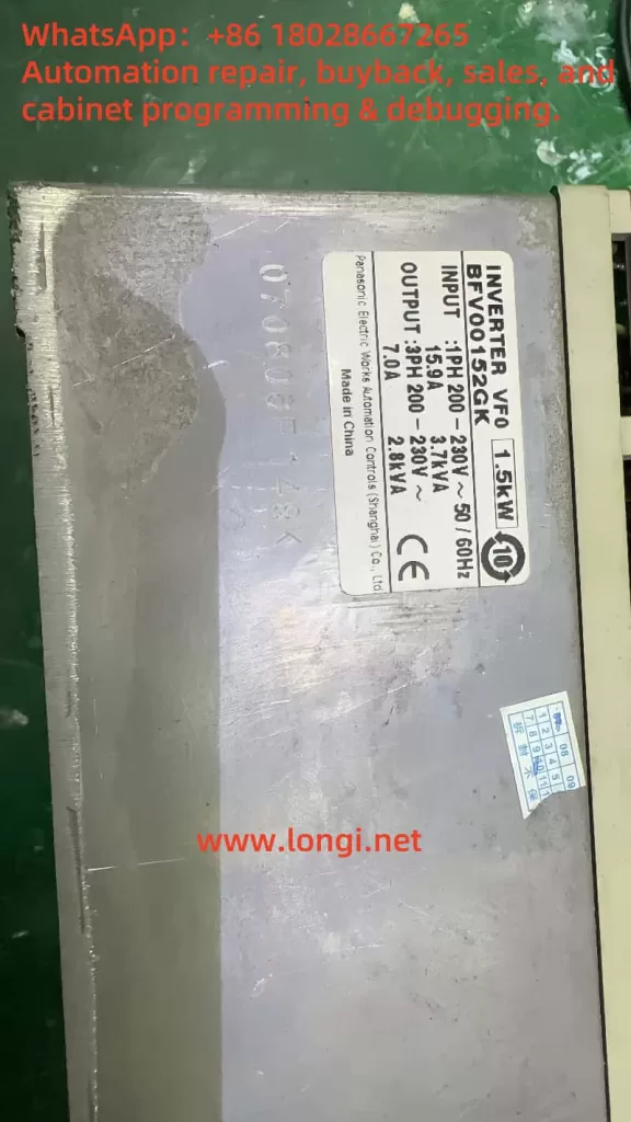
A Panasonic VF0 inverter (model BFV00152GK, 1.5kW) experienced frequent SC1 faults. On-site checks revealed:
- Internal fan failure
- Acceleration time set to only 0.5 seconds
- Enclosure internal temperature reached over 45°C
Fixes Applied:
- Replaced fan and cleaned heatsink
- Adjusted Pr.01 (acceleration time) to 3.0 seconds
- Added top exhaust fan to the control cabinet
Result: SC1 alarms were eliminated after these corrections.
5. Preventive Measures
To minimize SC1 alarms in the future:
- Periodically clean inverter and cabinet internals
- Replace consumables like fans and capacitors every 2–3 years
- Avoid aggressive acceleration settings
- Add temperature sensors and alarms for heat monitoring
- Use external torque/speed ramps for sensitive applications
6. Conclusion
The SC1 code on Panasonic VF0 inverters is a protection feature for acceleration-related overcurrent or thermal overload. It indicates a potential risk that should not be ignored. With proper diagnostics and control parameter tuning, SC1 alarms can be resolved efficiently, ensuring reliable and long-term operation of your automation system.