Exploring the Circuit Diagram and Maintenance Insights of the CONVO VSD Switch Power Supply
The CONVO VSD switch power supply, specifically designed for the GVF-G type drivers with a power rating of 5.5KW and version number 002-E-P00-01 8.6kVA 13A, presents an intriguing yet robust design in the realm of switch power supplies. Though it may not adhere to the most conventional designs, its performance in practical applications has proven to be reliable, with a notably low failure rate.

Circuit Overview
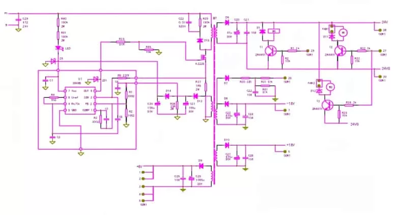
At the heart of this power supply lies an input stage that receives approximately 550V DC voltage from the autonomous DC home energy storage capacitor. This voltage serves as the foundation for the entire circuit’s operation. The oscillation and driving mechanisms are managed by the widely-used 38440 power chip, which initiates its operation through the voltage and current supplied by components R40, R41, and Z8. While the exact stabilization value of Z8 has not been precisely measured, it is estimated to be around 13V. An LED indicator is conveniently integrated to signal the presence of power.
Once the 3844 chip initiates oscillation, it establishes a power supply voltage for its 7-pin through rectification and filtering circuits comprising D13, Dl4, C30, and C31, facilitated by the BT winding. This power supply not only fuels the chip but also plays a crucial role in output voltage sampling and feedback. The sampled voltage, after being divided by resistors R1 and R2, is fed back to the 2-pin of the 3844 chip. This feedback method, which indirectly samples the output voltage of each channel rather than directly from the transformer’s secondary power supply branch, offers a unique approach albeit with slightly lower control precision and response speed.
Secondary Power Supply Enhancements
To further enhance the power supply’s performance, the +18V and -18V outputs from the secondary winding are routed to the CPU motherboard. Here, they undergo voltage regulation through 7815 and 7915 stabilizers, respectively. Although this adds a layer of complexity to the circuit, it significantly improves the power supply’s stability and reliability. Additionally, the +8V power supply, once introduced to the motherboard, undergoes 7805 voltage regulation to serve as the CPU’s power source.
Current Sampling and Control
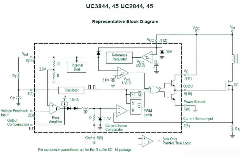
The switching tube’s current sampling is achieved through resistor R37, which is series-connected to the source of the K2225 switching tube. This sampled current is then sent to the 3-pin current detection terminal of the 3844 chip. The internal voltage amplifier’s feedback component, connected between the two pins, dictates the sampling voltage’s amplification rate. The 8-pin of the chip, known as the Vref terminal, outputs a stable 5V reference voltage during normal operation. This voltage provides a current path for the external R and C oscillation timing components connected to the 4-pin, ensuring the oscillation frequency’s stability.
The 6-pin of the 3844 chip serves as the pulse output or drive output terminal, introducing pulses to the gate of the K2225 switch through resistor R36. This meticulous control over the switching process is crucial for maintaining efficient and reliable power conversion.

24V Output and Fan Control
The 24V output power supply is versatile, providing both the control voltage for the frequency converter’s control terminal and powering two cooling fans. The fans’ operation modes are intelligently controlled by signals from the CPU motherboard, based on parameter settings. These modes typically include running upon power-on, running during operation, and running when the radiator temperature reaches a predefined threshold.
Maintenance Insights
When it comes to maintaining this power supply, several key points should be kept in mind. In the event of a breakdown-induced damage to the K2225 switch tube, a high voltage impulse can be introduced to the 3-pin of the 3844 chip, often leading to its simultaneous damage. Additionally, the R5 resistor may open or experience an increase in resistance value. Similarly, the current sampling resistor R37, connected to the source, is frequently found to be open. Therefore, a comprehensive inspection of these components is imperative before replacing the switch tube. As a direct replacement for the K2225, the K1317 tube can be used.
In conclusion, the CONVO VSD switch power supply, despite its unconventional design, offers a reliable and efficient solution for GVF-G type drivers. Its robust performance in practical applications, coupled with thoughtful design features and straightforward maintenance protocols, makes it a valuable asset in any frequency converter system. By understanding its circuit diagram and adhering to best maintenance practices, one can ensure the longevity and reliability of this power supply in various industrial and commercial applications.
