
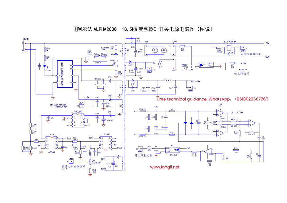
1.《Alpha ALPHA2000 18.5kW inverter》Switching power supply circuit diagram
The 530V power supply of the switching power supply is introduced from the CNPN terminal. The P terminal is added to the drain of the switching tube K2225 through the main winding of the switching transformer, and then to the N terminal through the emitter current sampling resistor, forming the input power supply path of the switching power supply. One path is added to the 6th pin of the oscillation board of the switching power supply (functional block diagram, including L3845P and other auxiliary components, see the second figure of the driving circuit for the specific circuit) through two 150kΩ2W resistors and the LED1 power startup circuit, providing excitation energy for the starting of the switching power supply. After the power supply starts oscillating, the self-powered winding of the switching transformer generates a DC power supply through rectification and filtering, which is input to pin 6 of the oscillation board as the power supply for the internal oscillation chip; pin 5 of the oscillation board is connected to the power supply N terminal, and pins 6 and 5 are the power supply pins of the oscillation board; the current sampling signal formed on the source current sampling resistor R39 of the switching tube is input to pin 3 of the oscillation board as a current control signal and a power supply stop protection signal. When an abnormal overcurrent occurs, the internal circuit forces the power supply to stop oscillating; the PWM controlled (variable pulse duty cycle) pulse is output from pin 4 of the oscillation board and connected to the gate of the switching tube to control the conduction and cutoff of the switching tube, so that the switching transformerinputs electrical energy and stores energy, and transmits the energy input by the power supply to the secondary load circuit in the form of electromagnetic transmission. The output voltage feedback signal of the switching power supply is input from pins 1 and 2 of the oscillation board, that is, the DC -15V voltage rectified and filtered by D48 and E28 outputs, which not only provides power for the CPU mainboard control circuit, but also serves as a feedback signal input to the oscillation board. Compared with the internal circuit reference voltage signal, an error voltage output is generated to control the PWM wave generator inside the oscillation board, so that the pulse duty cycle of the 4-pin input changes, adjusts the energy storage of the switching transformer winding, and maintains the output voltage unchanged.
The oscillation and voltage regulation of the switching power supply is to adjust the output voltage by changing the pulse width or period, which is called time proportion control. It is divided into two control modes: PWM (width modulation) and PFM (frequency modulation). The U3842, U3844, and U3845 series power supply chips are dedicated PWM controllers.
The switching transformer generates +11V power supply through rectification and filtering of the self-powered winding, and outputs 5V DC voltage through the 78L05C chip 8-pin voltage regulator to supply power to the input side of the U14-A7840 linear optocoupler. The U14 and LF513 two-stage amplifiers form the voltage detection circuit of the DC circuit. The DC voltage introduced from the P and N terminals is fed through a resistor divider network such as a 220kΩ 2W resistor and R54A to obtain a voltage value below 1V, which is then fed into the 2nd pin of A7840 through a 51Ω resistor . The voltage sampling signal output from the 7th and 8th pins of A7840 is fed into the input end of the differential amplifier (with an amplification factor of 1, which is actually a voltage follower for isolation and impedance transformation) composed of the subsequent LF353 through R55 and R56. The 1st pin of LF353 outputs a voltage signal that changes with the DC loop voltage, which is then compensated and adjusted by a semi-variable resistor and input into the subsequent circuit as a VPN (marked by the manufacturer on the circuit board, meaning the voltage sampling signal at the P and N terminals of the DC loop). When the input three-phase voltage is 380V and the DC circuit is about 530V, the VPN point voltage is about 3.8V .
by parallel rectification of D49 and D50 and 220μF50V current filtering is used as 1. Power supply for the cooling fan. The fan is put into operation when the inverter is powered on and there is no control; 2. Power supply for the control relay REL1 of the charging contactor coil. When the switch tube of the 1-pin of the wiring terminal CNN1 is turned on, REL1 is energized to control the charging contactor to be attracted; 3. Power supply for the module temperature detection circuit. The temperature sensor is a normally closed contact thermal relay, which is connected in series to the power supply branch on the input side of the photocoupler. When the module temperature rises abnormally, the temperature relay is activated, the normally closed point is disconnected, and the photocoupler outputs an OH overheat signal to the 14-pin of the CPU; 4. As the 24V power supply for the inverter control terminal. Other power supplies are omitted here.
The circuit on the lower side of the figure is a three-phase output voltage abnormality or three-phase output violent fluctuation or three-phase output phase loss detection circuit. This circuit form seems familiar to us. This circuit form of three-phase output voltage detection circuit has also been used in other inverters. At first glance, this is a typical instrument small signal amplifier, but it is not the case upon closer inspection. Due to the effect of the two input ends of the amplifier parallel diodes bidirectional clipping clamping, it means that the circuit no longer undertakes the task of amplifying small signals, but plays the role of shaping and synthesizing the input U and W two-phase signals into V-phase signals. Just like the principle of holography, if we look at it from the perspective of holographic theory, the U and W two-phase voltage signals must contain the information of the third phase V-phase voltage. Similarly, the synthesized V-phase signal contains the information of the U and V two-phase signals (in fact, the synthesized signal can be considered as the information of the three-phase voltage signal). I guess the subsequent circuit – the CPU’s internal hardware and software circuits is a circuit similar to a frequency meter, which counts the voltage wave heads input to the circuit. When it detects that a half-wave (or full-wave) of the three-phase output is missing, it determines that the output is missing a phase, and a fault alarm is given and the machine is shut down for protection.
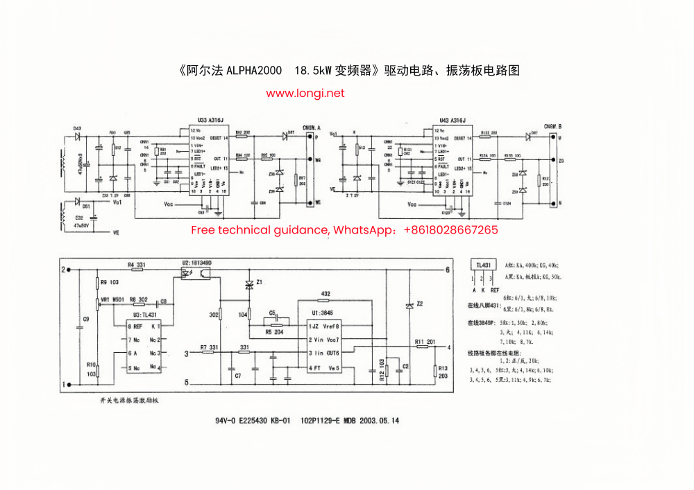
2.《Alpha ALPHA2000 18.5kW inverter》 drive circuit, oscillation board circuit diagram
To check the fault of the driver IC or IGBT module, you must know the principle of the A316J (HCPL-316J) protection circuit and the corresponding output state (level value) of the key functional pins. Let’s first look at how the internal and peripheral fault protection circuits of the A316J work. The figure shows the two-way drive circuit, and the remaining space is filled in here with the circuit inside the oscillator board of the switching power supply circuit, which is also mentioned in passing.
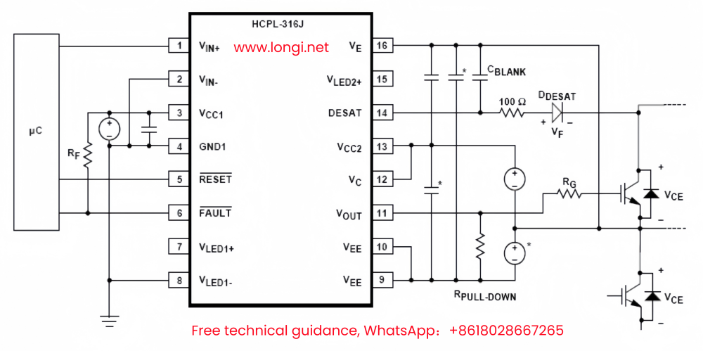
Combined with the above figure (a typical circuit in the A316J related information, it is easy to see the connection between the fault protection circuit and the IGBT), let’s talk about the action flow of the protection circuit. Readers, please first understand the power supply circuit and pulse output circuit on the input and output sides. This part depends on you to read it yourself. The space is limited.
Pin 14 of A316J is the module OC fault (overcurrent fault) detection input terminal, which is connected to the C pole of IGBT through an external 100 Ω resistor and an embedded diode, and pin 16 is connected to the emitter of IGBT. Pins 14 and 16 of A316J and the external circuit constitute the IGBT tube voltage drop detection circuit. Under normal working conditions, during the transmission of the drive pulse, the IGBT tube is reliably turned on, and the external diode of pin 14 is forwardly turned on due to the conduction of the IGBT tube, and the voltage value of pin 14 is embedded in the low (zero) level value of the voltage of pin 16. The internal fault detection circuit does not work, and the pulse transmission channel is unblocked. The internal circuit of pin 11 normally outputs the inverter pulse signal, and the module OC alarm signal output pin 6 also outputs a high-level signal under normal conditions; when the load current is abnormal, the inverter pulse signal path is poor, or the IGBT itself fails, causing the IGBT tube voltage drop to be greater than 7V, the external diode of pin 14 is reversely cut off, and a high-level signal appears between pins 14 and 16. The internal fault detection circuit is activated. On the one hand, the transmission of the pulse channel is blocked through the internal circuit, and on the other hand, the fault protection circuit is activated, so that pin 6 outputs a low-level module OC fault signal and sends it to the previous CPU circuit. When the IGBT has an overcurrent, the drive voltage output by pin 11 drops, causing the IGBT to softly shut down to avoid sudden shutdown caused by overvoltage caused by lead inductance and damage to the IGBT. When the internal IC power supply detection circuit detects that the input power supply voltage is higher than the internal reference voltage value and there is no overcurrent signal input, the pulse transmission channel works normally. If an undervoltage signal is detected, regardless of whether the pulse channel is transmitting normally, the internal fault protection circuit will be activated to turn off the upper tube (transmitting the driving voltage) of the push-pull output stage inside the A316J, and at the same time turn on the lower tube (transmitting the cut-off voltage) to softly turn off the IGBT.
After the module OC fault protection circuit is activated, the 6th pin of A316J will be locked in the low-level fault signal output state until a low-level reset signal is input from the 5th pin. An external circuit must output a fault reset signal to release the circuit lock state. The 14th pin is connected to an external embedded diode, and its working parameters have special requirements, reverse withstand voltage ≥ 1000V, turn-on time = 75ns. If ordinary diodes are used instead, the detection and protection function will be lost due to the charge storage effect of the junction capacitor, causing damage to the IGBT.
The oscillator board of the switching power supply is connected to the power supply/driver board through six pins. The -15V DC voltage output by the secondary winding rectification is input to the voltage stabilization control circuit of the oscillator board through pins 1 and 2. The voltage stabilization circuit consists of U3 (8-pin SMD TL431) reference voltage source and U2 (181349D) photocoupler. The change of -15V output voltage causes the change of input current of the light-emitting diode inside U2. The output internal resistance of the phototransistor on the output side of U2 changes accordingly due to the different amount of light received. This change signal is input to pin 2 of U1 (3845). The internal circuit of U2 controls the duty cycle of the output pulse of pin 6 of U2, and outputs the driving pulse to the gate of the switch tube through pin 4 of the oscillator board, controlling the on/off time ratio of the switch tube, thereby maintaining the output voltage of the secondary winding of the switching transformer within a certain value. The working current signal of the switching circuit is introduced into pin 3 of U1 through the R7 and C7 loop, and the internal circuit implements current closed-loop control and overcurrent protection.