Posted on Leave a comment

POWTRAN PI500 Series Current Vector Inverter: User Guide & Essential Features

This comprehensive guide covers the key features and essential operations of the POWTRAN PI500 Series high-performance current vector inverter, including parameter adjustment via the panel, start/stop control through terminals, external potentiometer debugging mode configuration, and multi-speed settings.

VFD panel operation method of POWTRAN

1. Adjusting Parameters via the Inverter Panel

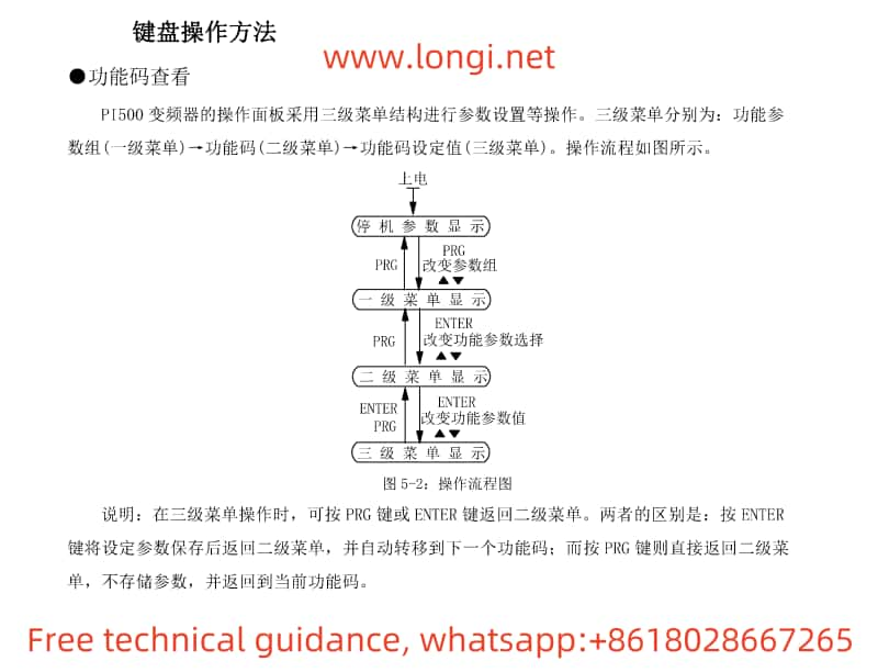
To adjust parameters using the inverter’s keypad, follow these steps:

  • Enter Menu: Press the PRG key to enter the parameter setting mode.
  • Select Parameter Group: Use the arrow keys to select the desired function parameter group (e.g., F0 group for basic function parameters).
  • Select Function Code: Within the selected group, use the arrow keys to choose the function code you wish to modify.
  • Adjust Parameter Value: Use the increment/decrement keys to adjust the parameter value or enter a new value directly with the numeric keys.
  • Save Settings: After making changes, press ENTER to confirm and save your settings.

Note: Some parameters cannot be modified during operation and require the inverter to be stopped first. Always consult the manual thoroughly before adjusting parameters.

Wiring Diagram of POWTRAN PI500

2. Starting and Stopping the Inverter via Terminals

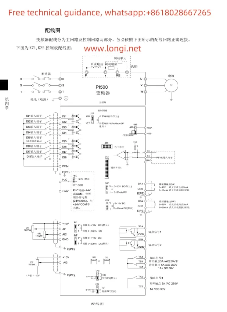
To control the inverter’s start and stop via external terminals, follow these configuration steps:

  • Set Command Source: Set F0.11 (Command Source Selection) to “1” (Terminal Control) to enable external terminal operation.
  • Assign Terminal Functions: Use F1 group function codes (e.g., F1.00, F1.01) to assign specific input terminals (e.g., DI1, DI2) for forward, reverse, stop, and other functions.
  • Wiring: Connect the external control signal wires correctly to the designated input terminals based on your settings.

To start the inverter, apply a closure signal to the forward terminal (e.g., DI1). To stop, apply a stop signal to the stop terminal (which may be DI2, depending on your configuration) or disconnect the forward signal.

External potentiometer analog quantity given wiring diagram of PI500

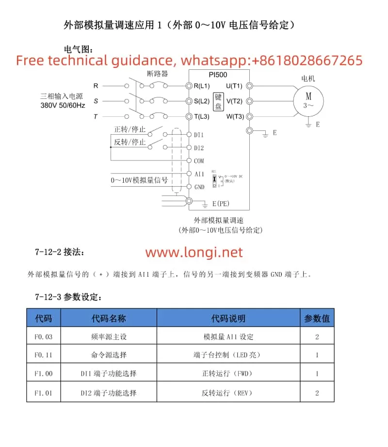
3. Setting External Potentiometer Adjustment Mode

To configure the inverter for external potentiometer adjustment, follow these steps:

  • Configure AI1 Input:
    • Wiring: Connect the external potentiometer’s output to the inverter’s AI1 and GND terminals.
    • Set Input Range: Adjust F1.12 (AIC1 Minimum Input) and F1.14 (AIC1 Maximum Input) based on the potentiometer’s output range to ensure the inverter interprets the signals correctly.
  • Select Frequency Source: Set F0.03 (Main Frequency Source Setting) to “2” (Analog AI1 Setting) to use the AI1 input signal as the frequency reference.
  • Start Adjustment: Once configured, rotating the external potentiometer will adjust the inverter’s output frequency.
Multi speed functional wiring diagram of PI500

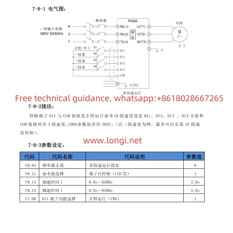
4. Introduction to Multi-speed Functionality

The multi-speed feature enables preset speed profiles, allowing quick switching between them via external signals.

  • Preset Speeds: Use E1 group function codes (E1.00 to E1.15) to set up to 16 different speed segments, each representing a percentage of the maximum frequency.
  • Assign Terminal Functions: Allocate input terminals (e.g., S1, S2, S3, S4) through F1 group function codes to select between the multi-speed segments based on their combinational states.
  • Set Acceleration/Deceleration Times: Customize acceleration and deceleration times for seamless speed transitions using parameters like F0.13 to F0.15.
  • Choose Speed Switching Method: Optionally, utilize external signals (high-speed pulses, communication signals) for dynamic speed segment switching.

To utilize the multi-speed feature, manipulate the allocated external terminals or transmit corresponding control signals. The inverter will then adjust its operating frequency according to the activated speed segment.

Notes:

  • Ensure speed segment settings align with the motor and inverter’s capabilities.
  • Carefully consider the mechanical load’s response to acceleration and deceleration when setting these times.

By following these configurations, you can flexibly manage the inverter’s speed to meet various process demands, while also benefiting from the manual’s detailed guidance for troubleshooting and maintaining optimal performance.

To learn more about the usage of PI500 VFD, you can download its manual from Google Drive or contact our service:https://drive.google.com/file/d/1zCUn1w6h9rEkvbP0yPJ1qAA5–T7axBt/view?usp=sharing

Posted on Leave a comment

Application of S87C196MH (MC) microcontroller in inverter mainboard

1. Pinout of the 80-pin S87C196MH (MC) microcontroller in SMD package:

2. Introduction to the structure and functions of the S87C196MH (MC) microcontroller:

The controller is a 16-bit microcontroller produced by Intel. It is widely used in inverter products due to its powerful functions and high versatility.

The internal circuit includes arithmetic logic unit (RLU), registers, internal A/D converter, PWM generator, event processing array (EPA), three-phase to complement SPWM output generator, watchdog, clock and interrupt control circuits, etc. The internal structure schematic is as follows:

 The S87C196MH (MC) microcontroller uses CHMOS technology, has an operating temperature of -40 º C–85 º C, supports 16KB EPROM, and when the crystal oscillation frequency is 16MHz, it only takes 1.75 μs to complete 16-bit by 16-bit multiplication . It is suitable for the rapidity requirements of the control system. There are 7 I/O ports, and each port pin is multifunctional.

The register array has 512B, which is divided into low 256B and high 256B. The low 256B can be used as 256 accumulators during ALU operation, and the high 256B is used as register RAM. The high 256B can also be switched to 256B with accumulator function through unique window technology. The microcontroller has 13 10-bit/8-bit high-speed A/D converters inside, and the conversion time can be set between 1.39-40.2 μs . The A/D can also be used as a programmable comparator to generate an interrupt when the input crosses a threshold level.

The event processing array (EPA) mainly performs input and output functions. In input mode, the EPA monitors the changes in the input pin signal and records its time value when the event occurs. This process is called capture. In output mode, when the timer matches a stored time value, the output pin is set, cleared or triggered. Both capture and compare events can generate normal service processes or interrupts. There are 4 capture/compare modules and 4 compare modules.

EPA also contains two 16-bit bidirectional timer/counters T1 and T2. T1 can be timed according to an external clock source. In this working mode, EPA can directly process two pulse signals with a 90 ° phase difference output by the position sensor (such as a photoelectric encoder) to monitor the speed and direction of the motor.

External event processing server (PTS). The controller has two types of interrupt systems: programmable interrupt controller and PTS. The programmable interrupt can be set to PTS interrupt service mode. PTS has several micro-instruction coded hardware interrupt service processes, which can work in parallel with the CPU and can complete data block transfer, process multi-channel A/D conversion, control serial communication and other functions.

The S87C196MH (MC) microcontroller has a three-phase complementary SPWM waveform generator built in, which directly outputs six SPWM signals through the P6 port. The driving current can reach 20 mA and the driving frequency can reach 8MHz. Each SPWM signal can be independently programmed and the dead zone interlock time can be set.

3. Application of S87C196MH (MC) in INVT inverter motherboard:

(1) Power supply, clock, reset, etc. Pins that meet the basic working conditions of the microcontroller.

(2) Pins for processing digital and analog signals at the control terminals. The start, stop and speed control of the inverter, as well as the monitoring of the working status, are all carried out through the control terminals. The input and output signals of the control terminals directly enter the microcontroller pins.

The output of the analog signal of the inverter control terminal actually comes from the PWM0 (P6 I/O port) pin of the microcontroller. The actual output is a width-modulated pulse signal, which is converted into an analog voltage signal by the subsequent circuit.

(3)Switching control signal, control of charging contactor (relay control), control of cooling fan and reset control of drive circuit (release its fault lock state).

  (5)Processing of various detection and protection signals:

(6) Processing of other functional pins

Some pins are connected to ground, +5V, or +5V via a pull-up resistor according to their functions. Some pins are left unused.

    The specific functions of each pin of the S87C196MH (MC) microcontroller have been explained in detail above. In troubleshooting, the cause of the fault can also be determined and the fault location can be found based on the level status of the relevant pins.

For example, if the signal input of a certain terminal of the inverter is invalid, measure whether there is a 0-5V voltage change on the corresponding pin of the CPU , and then quickly determine whether it is a terminal input circuit fault or a CPU fault.