
In-depth Analysis and Maintenance Guide for Mitsubishi F1S Switching Power Supply
In the field of modern industrial automation, the application of Mitsubishi PLCs (Programmable Logic Controllers) is extensive. As a critical component of PLCs, the stability and reliability of the switching power supply directly determine the operating efficiency of the entire system. This article takes the Mitsubishi F1S switching power supply as an example, deeply analyzing its circuit structure, working principle, and maintenance methods. The aim is to provide readers with a comprehensive and practical technical guide.
I. Overview of Circuit Structure
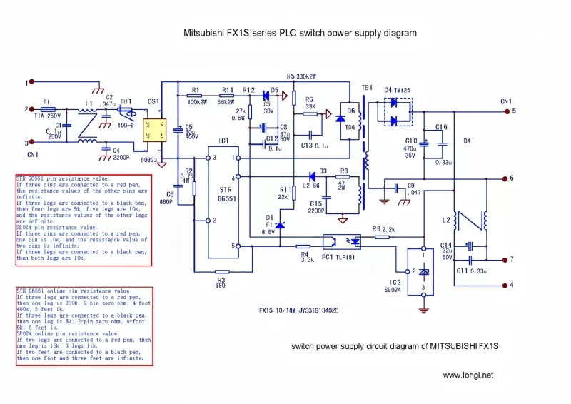
The Mitsubishi F1S switching power supply board is designed intricately, featuring two relatively independent 24V output structures (although somewhat isolated by L2, they can still be considered as two separate outputs). These two outputs not only provide stable 5V power supply for the PLC motherboard but also offer DC24V external control power for external measurement instruments and other devices. The power board is tightly connected to the motherboard through copper needle-shaped rigid wires, ensuring stable signal transmission.
II. Detailed Explanation of Working Principle
- Input Filtering and Protection: After entering the power board through the L and N terminals of the PLC, the industrial frequency 220V power first passes through a bidirectional low-pass filter network composed of C1, C2, C4, and L1. This design effectively filters out high-frequency interference and improves the purity of the power supply. Meanwhile, the bidirectional filters L1 and L2 further isolate high-frequency interference pulses from both inside and outside the power supply, ensuring stable system operation. F1 serves as an overload protection fast-acting fuse, while TH1 acts as a temperature fuse, together constituting a dual protection mechanism for the power supply.
- Rectification and Oscillation: The filtered AC power passes through F1 and TH1 into the full-wave rectification circuit, where it is rectified to obtain a direct current voltage of approximately 280V. This voltage is sent to the oscillation and voltage-stabilizing circuit centered on STRG6551. STRG6551 is a power oscillation module with an integrated switching tube. Its 4 and 3 pins are the power supply terminals, while 1 and 2 pins are internally connected to the source and drain of the power switching tube. Additionally, pin 2 provides negative feedback for the switching operating current. Pin 5 is the feedback voltage input terminal, used to regulate the stability of the output voltage.
- Voltage Stabilization and Protection: The voltage induced by the secondary winding of the switching transformer TB1 undergoes rectification and filtering before serving as the working power for the PLC. To maintain voltage stability, the system employs an output voltage sampling circuit composed of R9, IC2, PC1, and other components. When the voltage changes, this change is converted into a variation in the input current on the PC1 optocoupler device, which is then fed into pin 5 of STRG6551 through R4. The comparison amplification circuit inside STRG6551 adjusts the conduction/cutoff time of the switching tube, i.e., controls the duty cycle of the oscillation frequency, to achieve stable output voltage.
Furthermore, the system boasts a comprehensive protection mechanism. When an abnormal load causes a sharp increase in current, the voltage variation across the sampling resistor R2 is introduced into pin 5 of STRG6551, reducing the output voltage to decrease the load current. When the voltage or current anomaly reaches a certain threshold, STRG6551 disconnects the driving circuit of the switching tube, causing the circuit to oscillate and protecting the subsequent circuit from damage.
III. Maintenance Methods and Practices
Faced with potential faults in the Mitsubishi F1S switching power supply, reasonable troubleshooting steps and scientific maintenance methods are crucial for improving maintenance efficiency. Here are some common maintenance methods:
- Routine Inspection: First, check whether the F1 and TH1 fuses are blown. If they are blown and there are no abnormal short-circuit points in the switching tube and load circuit, replacing the fuses generally resolves the issue. If the power still does not oscillate after replacing the fuses, further investigation is needed.
- Identify Fault Circuits: Disconnect the PLC motherboard, use a voltage regulator to adjust the input voltage to below AC100V, and connect a dummy load (such as a 100Ω 5W resistor). Short-circuit pins 1 and 2 of the PC1 optocoupler to make the voltage feedback signal zero. Power on and observe the power output. If there is output but not at a stable voltage, the fault lies in the voltage-stabilizing circuit; if there is no output, the fault is in the oscillation circuit.