
1. The difference between various types of driver ICs:
The core component of the inverter drive circuit is the driver IC, and the commonly used models are TLP250, A3120, PC923, PC929, A316J, etc. The driver IC is essentially a type of optocoupler device. The purpose of using optocouplers is to achieve isolation of different power supply circuits on the input and output sides of the coupling, and to ensure that the output side has a certain power driving capability, which has both electrical isolation and power amplification.
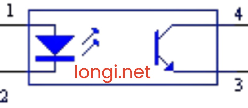
Ordinary four-wire end optocoupler devices, such as PC817, have an internal circuit consisting of an input light-emitting diode and an output photosensitive transistor. After the input current (typical application value 5-10mA) is passed through the input side , the output side transistor generates excited photoelectrons and conducts. This type of optocoupler is mainly used for the transmission of switching signals, such as the digital signal control terminal of the inverter.
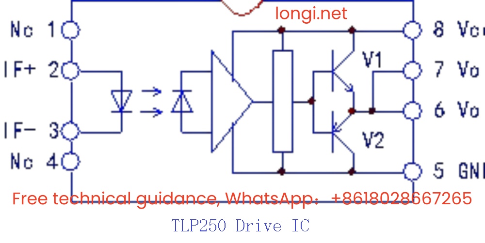
As an optocoupler device of the driver IC, its structure is slightly more complicated than that of PC817. The output stage is mostly composed of emitter output to the complementary amplifier, such as TLP250, A3120, PC923, etc. The output stage is composed of two-stage emitter complementary circuits, V1 and V2. When V1 is turned on, the VCC positive supply voltage is added to the gate-emitter junction of the IGBT through the output pins 6 and 7, providing the driving current for the IGBT to turn on. If the gate-emitter junction of the IGBT is regarded as a capacitor, the V1 conduction provides the charging current of the gate-emitter junction capacitor of the IGBT to turn it on; and when V2 is turned on, the output pins 6 and 7 are pulled to the GND ground level or the negative supply voltage, providing a charge discharge channel for the gate-emitter junction capacitor of the driven IGBT, so that it is quickly cut off. During work, V1 and V2 are alternately turned on to implement the on and off control of the IGBT. It should be noted that the power supply for this drive circuit often uses a positive and negative dual power supply of +15V and -7.5V to enhance its control ability.
PC929 adds IGBT protection circuit, also known as IGBT conduction tube voltage drop detection circuit, based on the circuit structure of TLP250, A3120, PC923, etc., which is mainly responsible for the rapid protection of IGBT from overcurrent and short circuit. As we all know, in the U, V, W output circuit of the inverter, two or three current transformers are connected in series (the current signal is collected by the Hall element and processed by the amplification circuit), and the output signals are processed into analog and switch signals by the back-stage circuit respectively, and sent to the CPU for current display, output control, automatic speed control and current limiting control and overload protection during startup and operation. However, the current transformer circuit often has a large time constant and cannot implement μs -level rapid protection for IGBT. In fact, the implementation of overload and short circuit protection for IGBT depends on driver ICs such as PC929 and A316J to a certain extent.
Because the tube voltage drop when the IGBT is turned on actually reflects the working state of the IGBT, the overcurrent detection of the IGBT can be implemented by using the IGBT’s energy-conducting tube voltage drop signal, which can effectively implement the rapid overcurrent protection of the IGBT. The IGBT tube is an organic combination of a two-stage device and a field-effect device. The collector and the emitter form an output current path and have a certain conduction internal resistance. When the IGBT works within the rated current, the normal conduction tube voltage drop should be less than 3V. When the overcurrent is nearly 2 times, the overload current forms a large voltage drop on its conduction internal resistance, causing the tube voltage drop to rise to about 7V. Since the overload capacity of electronic devices is poor, the overload time allowed is short, and the faster the protection action, the better. Detecting the IGBT’s conduction tube voltage drop signal to cut off and protect the IGBT has become the most effective and widely used method in the inverter drive circuit.
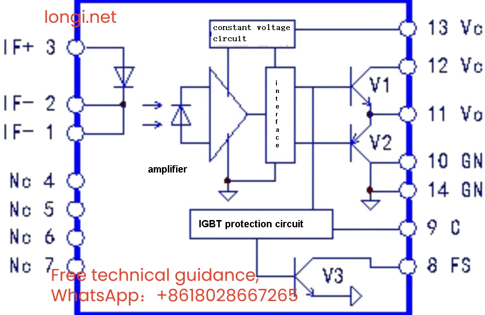
Compared with PC923, PC929 (pictured above) has an additional IGBT protection circuit. Pin 9 is connected to the C and E poles of the driven IGBT together with the external components to detect the IGBT conduction tube voltage drop signal. When the tube voltage drop signal rises to above 7V due to overcurrent, the internal triode V3 of pin 8 is turned on, and the OC and SC signals are isolated by the external optical coupler and sent to the CPU. The inverter reports the OC signal and shuts down for protection. (For details, please refer to the article “Repair of PC923 and PC929 drive circuits”)
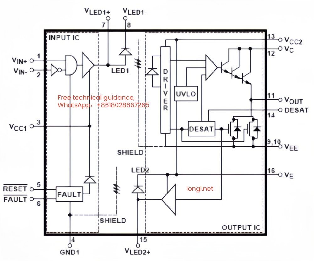
However, it can be seen from the circuit structure of PC929 that V3 of the OC alarm circuit is directly electrically connected to the output side circuit, which is the strong current side. The OC signal can only be sent to the CPU through optocoupler isolation. Assuming that the optocoupler that transmits the OC signal is also integrated into the driver IC, the OC signal output pin of the driver IC can be directly connected to the CPU pin. Then the A316J in the driver IC can complete this task.
The internal circuit structure of A316 is shown in the figure below. The PWM pulse signal from the CPU is input through pins 1 and 2, isolated by the internal photocoupler LED1, the interface circuit and the power output circuit, and output from pin 11 to drive the IGBT; the external components at pins 14 and 16 and the internal circuit constitute the IGBT tube voltage drop detection circuit. When the IGBT protection circuit is activated, the LED2 photocoupler transmits the OC signal to the input side, which is output from pin 6 and sent to the CPU.
Compared with other driver ICs, A316J has the following two features:
(1) The input side is not a light-emitting diode, but a digital gate circuit. It does not need to draw a large original drive circuit from the signal source. The input impedance is high and it is easy to connect directly to the CPU pin, eliminating the intermediate drive circuit link.
(2) After the OC signal fault occurs, there is a fault lock function, which blocks the transmission of the pulse signal. Only after a low-level reset signal is input from pin 5, can the fault lock state be released and the pulse transmission path be opened. Therefore, A316J also has a fault reset function.
In this sense, A316 is an integrated driver IC with the most complete control functions.
2. Methods for removing OC fault alarm
During maintenance, we often need to disconnect the drive circuit from the main circuit for separate inspection. At this time, the OC fault alarm function of the drive circuit will cause us a little trouble. When the drive board is powered on separately, the operation panel often reports an OC fault, making it impossible for us to detect whether the drive circuit is normal.
It is necessary to take corresponding measures to release the OC fault alarm function of the drive circuit to facilitate the inspection of whether the drive circuit can transmit six-channel drive pulses normally.
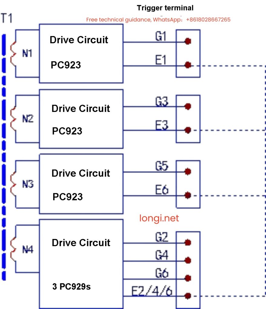
In the drive circuit, PC923 and PC929 often appear in pairs, and PC929 is responsible for detecting the voltage drop of the lower three-arm IGBT conduction tube, and reports the OC signal to the CPU when a fault occurs. When the drive board is disconnected from the main circuit IGBT, it is equivalent to the IGBT open circuit. Once the start signal is sent, PC929 will send an OC signal to the CPU.
pulse trigger terminals E1 – E6 (dashed lines in the figure below) to artificially create the false appearance of “normal opening” of the three-arm IGBT in the inverter circuit. PC929 no longer returns OC signal to the CPU, so the CPU outputs six pulse signals to six driver ICs, so that you can check whether the drive circuit is normal.
The A316J driver IC can also detect the voltage drop of the upper three-arm IGBT and report the OC signal. See the figure below:
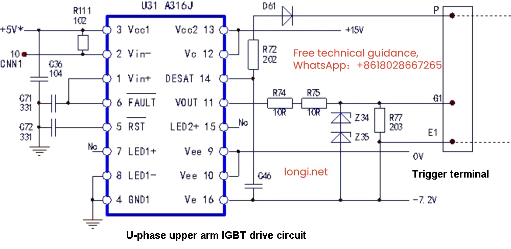
By short-circuiting the trigger terminals P and E1, the “conditions” for turning on the IGBT are artificially created, thus releasing the OC fault detection and alarm function of A316J.
The method of removing the OC alarm function of the three-arm IGBT drive circuit of A316J is the same as above. See the figure below:
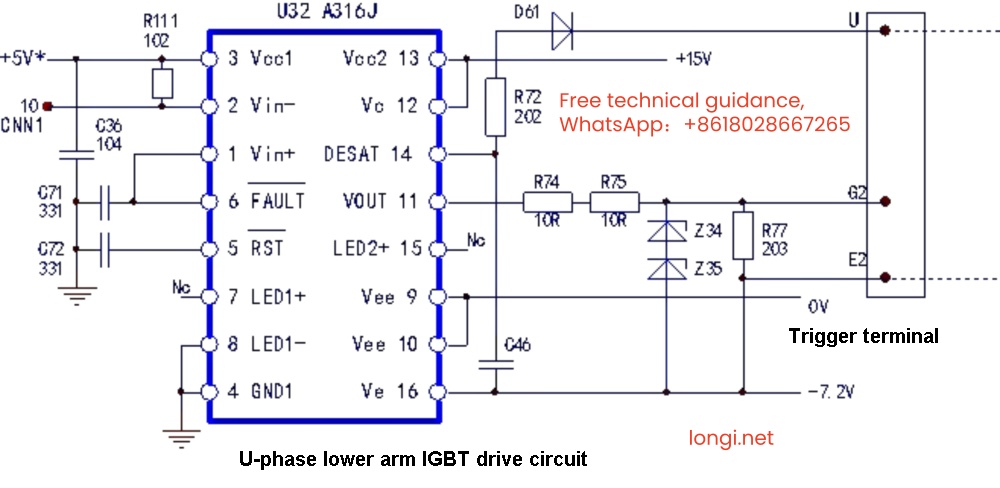
The driving circuit of the U-phase lower arm IGBT can short-circuit the U and E2 contact terminals, thereby releasing the IGBT tube voltage drop detection and OC signal alarm functions.
There are two points to note:
(1)For the detection of the voltage drop of the lower three arms or the lower three arms IGBT tubes separately, the trigger terminals of the upper three arms or the lower three arms can be short-circuited to release the OC alarm function. For the detection of the voltage drop of all six IGBT tubes, only the trigger terminals of the upper three arms IGBT can be short-circuited, and the OC alarm of the lower three arms can only be released by using a fine needle to pick up the 6th pin of A316; after checking that there is no problem with the upper three-arm drive circuit, remove the short-circuit line, pick up the 6th pin of the upper three-arm drive IC, short-circuit the trigger terminal of the lower three-arm drive circuit, and check whether the lower three-arm drive circuit is normal;
(2)If the trigger terminal has two pins, only G2 and E2, you should find the cathode of diode D61 from the 14 peripheral circuit of A314J, short-circuit it with E2, and release the OC alarm function.
Most of the maintenance of the inverter is the maintenance of the drive circuit. After the drive circuit is repaired, the power-on test of the inverter circuit must be cautious! ! You should use measures such as series light bulbs, 2A fuses, and DC low voltage. After confirming that the inverter circuit is fault-free, restore the 530V DC power supply.