
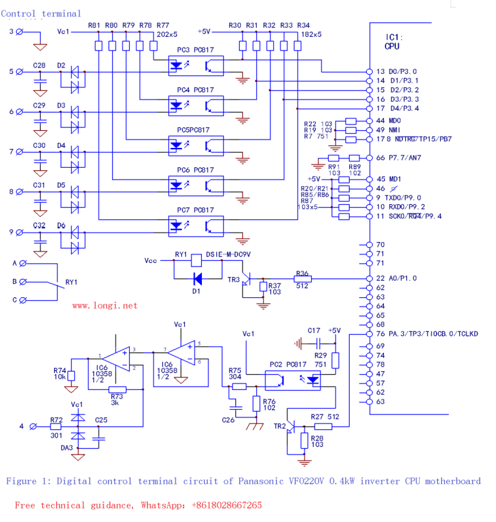
1. Digital control terminal circuit:
The operation control terminal of the frequency converter receives, outputs and processes two types of signals: digital and analog. Analog signals are generally used to input frequency instructions of 0-5V (10V) to determine the output speed of the frequency converter; output analog voltage signals corresponding to the output (given) frequency for external frequency meters to display the operating frequency, etc. The input signals of digital signals are used for the start/stop and fault reset of the frequency converter; the output switch signals are used for external relays and indicator lights to monitor the fault or operating status of the frequency converter, etc.
The following figure (Figure 1) is a digital control terminal circuit, 3 is a digital signal common terminal, 5, 6, 7, 8, 9 are digital signal input terminals. When any of the signal input terminals is connected to the common terminal 3, it can form an input path of the optocoupler, thereby transmitting the control signal to the CPU. The benefit of using optocouplers is that in addition to achieving electrical isolation, it also improves the anti-interference performance. The signals of the inverter control terminal, both input and output, are directly from the CPU pins. Pins 13 to 17 of the CPU are the switch control signal input pins. Pin 22 outputs the switch signal, and the signal content (operation, fault, etc.) can generally be set by parameters, also known as the programmable output terminal. The output signal provides a forward base bias current for the control switch tube TR3 through R36. The conduction of TR3 directly drives the RY1 relay, and the switch signal is output from the three terminals A, B, and C for the external indicator light or relay to indicate the working status of the inverter.
The output from the 76th pin of the CPU is a pulse signal representing the output speed, which drives the transistor TR2 through R27, and TR2 drives the optical coupler PC2. The pulse signal output by PC2 is filtered into a smooth DC voltage by R75 and C28, and is added to the subsequent two-stage voltage follower for current amplification, and then outputs a 0-10V (frequency output) analog signal from the control terminal 4. This circuit can actually be regarded as a simple analog/digital conversion circuit. Although the terminal output is an analog voltage, the CPU output is still a digital (pulse) signal.
For digital (switching) signals, at any time, the input and output potentials of the circuit are both in two states: 0 (ground potential of the power supply) and 1 (positive terminal potential of the power supply).
The following figure ( Figure 2 ) is still part of the control terminal circuit. Because the four bidirectional analog switch circuits of IC4 (BU4066BCK) are used for unified input and output processing, the digital/analog circuits are drawn together for ease of reading. IC4 can transmit digital and analog signals. It contains four sets of bidirectional switches. Each set of switches has an independent on/off control terminal CTL. When the terminal is at a low level, the switch is in the off state, and the I/O and O/I are in a high impedance state; when the CTL terminal is at a high level, the switch is in the on state. The purpose of using a bidirectional analog switch is to make the transmission of the signal controlled by the CPU instruction, thereby realizing programmable input and output control. The circuit switches the input of two input signals and switches the output of two digital signals.
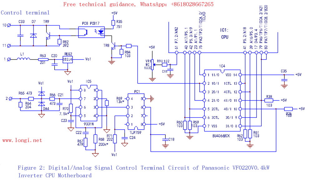
For the switching control of the two input analog signals, in order to facilitate the principle analysis, the analog signal path in the circuit of Figure 2 is redrawn as follows:
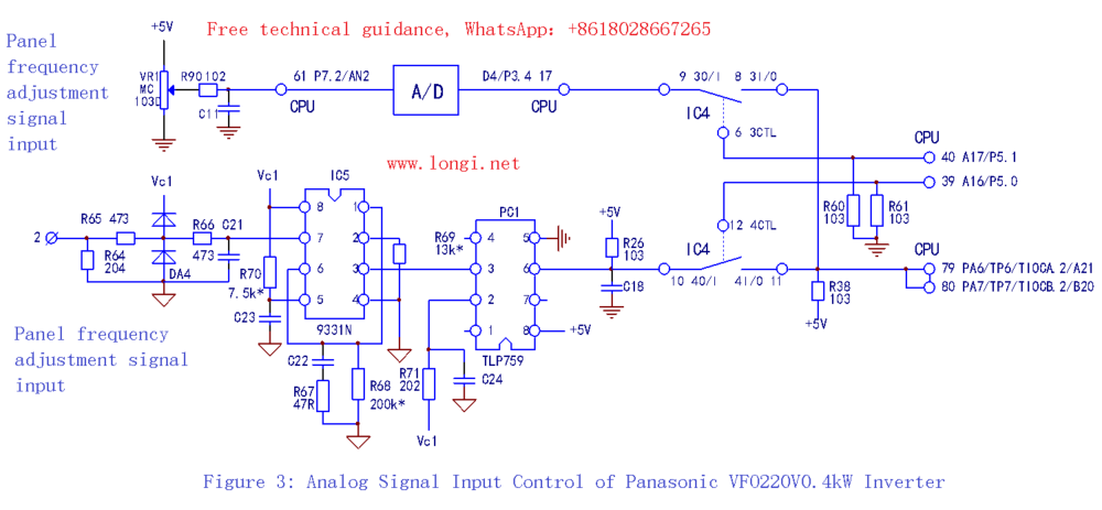
Panel frequency command circuit: VR1 is a potentiometer on the operation display panel, which can adjust the inverter output frequency from the operation panel. The adjustment voltage of VR1 is input to the 61st pin of the CPU through the R90 and C11 anti-interference circuits, and after internal A/D conversion, it is output from the 17th pin, through the IC4 bidirectional analog switch, and connected to the 11th pin of IC4, and then input to the 79th and 80th pins of the CPU;
Terminal frequency command circuit: The control terminal 2 inputs the variable voltage signal of the center arm of the external potentiometer, which is first converted by IC5 (93321N) into a U/F signal and then converted into a frequency signal proportional to the input voltage. It is then sent to another set of bidirectional analog switches inside IC4 through the PC1 (TLP759) photocoupler and output from pin 11.
The two frequency command signals are controlled by the level states of the CPU’s 39 and 40 pins, and further controlled by the user’s control intention. The control parameters can be set. When the 40 pin is high and the 39 pin is low, the CPU inputs the frequency command from the operation panel and determines the output frequency accordingly; otherwise, the control terminal is connected to an external potentiometer (or other analog voltage control signal, such as an instrument output signal, etc.) to adjust the output frequency.
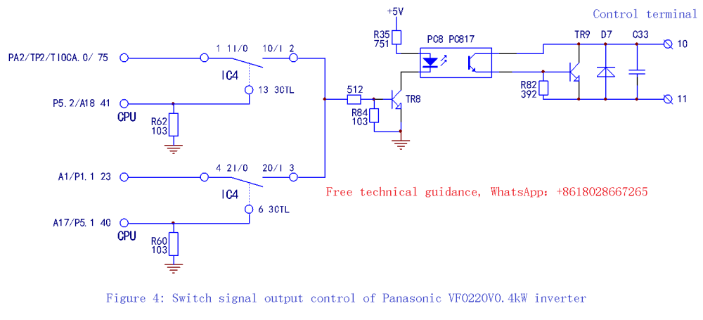
Control terminals 10 and 11 are open collectors, and the switch signal output can realize programmable output. The user sets the output content through parameters, or the terminal is connected during operation, or the terminal is connected during failure. Under the control of the CPU’s 41-pin output instruction, when the analog switch 1 and 2 are connected, the photocoupler PC8 is driven by TR8 and turned on, and the terminals 10 and 11 are in a low-resistance state, outputting an operation signal; when the analog switch 3 and 4 are connected by the CPU’s 40-pin output instruction, the terminals 10 and 11 are also in a conducting state, but the output at this time is the inverter fault signal.
Similarly, the content of the output signal depends on the user’s intention – the CPU’s instructions. The two sets of analog switches play the role of a two-throw switch. Different output contents are switched according to the user’s intention.