The main circuit of the inverter is a voltage-type, AC-DC energy conversion inverter. Since there is a large-capacity capacitor energy storage circuit between the rectifier and inverter circuits, and the voltage across the capacitor cannot change suddenly, in the initial power-on stage, the capacitor device is equivalent to a “short circuit”, which will form a huge surge charging current, which will cause a large current impact on the rectifier module and cause it to be damaged, and will also cause the air circuit breaker connected to the inverter power supply end to trip due to overcurrent.
The conventional processing method is to connect a current limiting resistor and a charging contactor (relay) in series between the rectifier and the capacitor energy storage circuit. The control of the capacitor charging process is as follows:
When the inverter is powered on, the charging resistor first limits the current of the capacitor to suppress the maximum charging current. As the charging process extends, the charging voltage gradually builds up on the capacitor. When the voltage amplitude reaches about 80% of 530V, two control processes occur. One is that the switching power supply circuit of the inverter starts to oscillate. The 24V output of the switching power supply directly drives the charging relay, or the relay connects the coil power supply circuit of the charging contactor. The charging contactor (relay) is closed. When the charging current limiting resistor is short-circuited, the inverter enters the standby working state. After a certain voltage is established on the capacitor, its charging current amplitude is greatly reduced, and the closing/switching current of the charging contactor is not too large. After that, the power supply of the energy storage capacitor circuit and the inverter circuit is supplied by the closed contactor contacts, and the charging resistor is short-circuited by the normally open contact of the contactor. The second is that as the charging voltage on the capacitor is established, the switching power supply starts to oscillate, and the CPU detects the voltage amplitude signal sent by the DC circuit voltage detection circuit, determines that the charging process of the energy storage capacitor has been completed, and outputs a charging contactor action instruction. The charging contactor is powered on and closed, and the capacitor charging process ends.
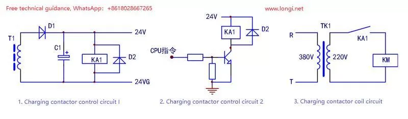
The common main circuit forms of the inverter and the charging contactor control circuit are shown in the figure below:
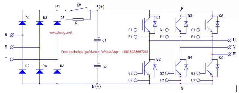
For some inverters and high-power inverters, the rectifier circuit often adopts a three-phase half-controlled bridge circuit, that is, the lower three arms of the three-phase rectifier bridge are rectifier diodes, and the upper three arms use three unidirectional thyristors, using thyristors as “contactless switches” to replace charging contactors. This saves installation space and improves circuit reliability. The circuit form is shown in the figure below:
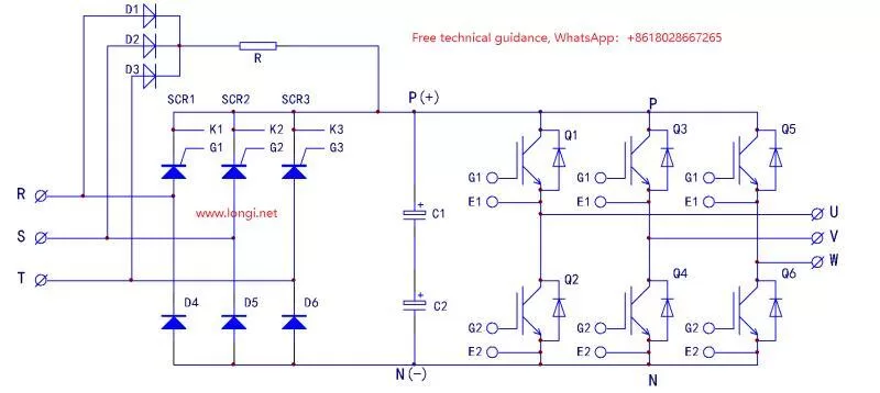
Although the charging contactor is omitted, the working principle is the same, but the control circuit is different. During the power-on period of the inverter, D1 ∽ D6 is used for rectification, and R is used for current limiting to charge C1 and C2. When the charging process is close to the end, the CPU outputs the opening instruction of the three thyristors SCR1 ∽ SCR3, and the control circuit forces the three thyristors to conduct. The power-on pre-charging circuit composed of D1, D2, D3, and R is used. SCR1 ∽ SCR3 and D4, D5, and D6 form a three-phase rectifier bridge. At this time, the thyristor is in a fully conductive state, which is equivalent to a rectifier diode.
The opening of the thyristor requires two conditions: 1. The positive voltage between the anode and the cathode; 2. A trigger current loop is formed between K and G. The circuit is connected to the three terminals of the AC input power supply to provide unidirectional controlled rectification. During the three positive half-wave voltages of the three-phase AC power, if the trigger current is formed at the same time, the three thyristors can be opened. The first condition has been formed naturally, and the second condition is sufficient to control its opening.
To put it simply, as long as a trigger current (pulse or DC) is provided to the thyristor during the period when the thyristor is subjected to a forward voltage – when the AC voltage passes through zero, the thyristor can be turned on well during the positive half-wave of the AC power and rectify the input AC voltage (just like a diode). The simplest trigger circuit is to introduce a resistor from the anode to the G pole, and during the positive half-wave of the AC power (after the zero point), the trigger current is synchronously introduced to the thyristor to turn on the thyristor. For example, the main circuit form of Dongyuan 300kW inverter is the same as Figure 3, and the trigger circuit is relatively simple:
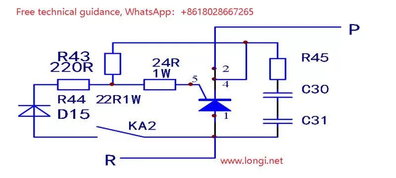
Figure 4 is one of the thyristor trigger circuits. The other two trigger circuits are the same. The components R45, C30, C31 and other components connected in parallel at the anode and cathode of the two thyristors are peak voltage absorption networks to provide overvoltage protection for the thyristors. The KA2 contact, D15, R44, and 24R form a trigger current path. The function of D15 is to rectify the input voltage half-wave to prevent the thyristors G and K from being subjected to the impact of reverse trigger voltage/current. R44 and 24R are current limiting resistors to limit the peak trigger current and protect the safety of the thyristors. R43 is a noise elimination resistor to increase the reliability of the thyristor operation.
When the CPU issues a thyristor on command, relay KA2 is powered on and closed, a positive half-wave voltage is input, rectified by D15, limited by R44 and 24R, flows into the G pole of the thyristor, and flows out from the K pole, forming a trigger current path, and the thyristor is turned on. The thyristor in the circuit is not in the voltage regulation working area, the conduction angle is the largest, and it is in the “full conduction state”, just like a switch device, only in the two states of conduction and cutoff, without the third state of phase shift (voltage regulation). This is where attention needs to be paid. Therefore, the control circuit is different from the conventional phase shift control circuit and is relatively simple.
A slightly more complex thyristor control circuit, such as the trigger circuit of the Delta 37kW inverter thyristor, is shown in the figure below:
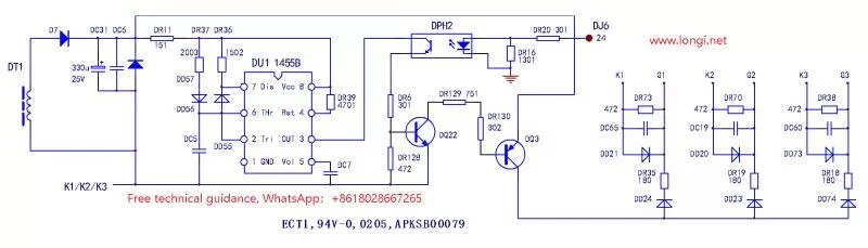
After rectification and filtering by an independent power supply winding of the switching power supply, it is used as the power supply for the thyristor trigger circuit. The control circuit consists of the NE555 time base circuit, the DPH2, DQ22, DQ3 trigger pulse on/off circuit, and the D and R three-way trigger flow circuit. After the switching power supply works, the NE555 time base circuit is connected to a multi-resonance oscillator and is powered on. Whether the oscillation pulse output from pin 3 is sent to the three trigger circuits of the subsequent stage depends on the command control of the CPU. The command signal of the CPU is introduced to the input side of the photocoupler DPH2 through the 24th pin of the control wiring terminal DJ8. When the transistor on the output side of the optocoupler is turned on, the pulse signal of the NE555 oscillator is sent to the D and R trigger circuit loop of the subsequent stage through the transistors DQ22 and DQ3. After the CPU issues the thyristor opening command, the three devices DPH2, DQ22, and DQ3 are always in the on state, and the trigger pulse is always added to the G and K of the three thyristors. The peak trigger current is about 100mA.
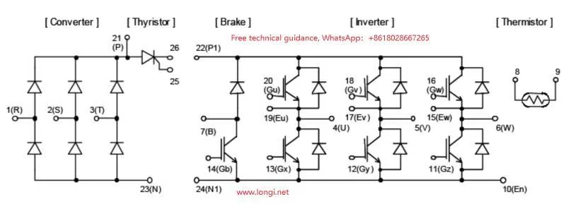
In addition, in the Panasonic and Fuji small power inverter models, another form of main circuit structure is used to complete the initial charging control of the main circuit capacitor. This is the internal circuit structure diagram of the 7MBR35SD120 integrated power module. The circuit is shown in Figure 6:
The difference of the circuit is that a controllable device is added after the three-phase rectifier bridge. A charging resistor must be connected in parallel to the terminals 21 and 26. After a certain charging voltage is established on the main circuit capacitor, a trigger current is input from terminals 25 and 26, then the thyristor is turned on and the inverter enters the standby working state.
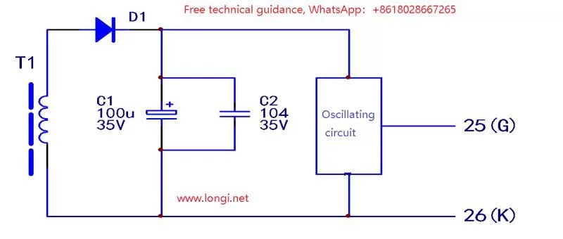
The control circuit is generally powered by an independent 24V winding of the switching transformer to obtain control power with a “floating ground”. The control circuit is mostly an oscillation circuit, which increases the pulse trigger current of the thyristor device. The oscillation circuit is not a conventional phase-shift trigger circuit, but provides high-frequency/density random trigger pulses to put the thyristor in a fully conductive state. The thyristor here, under the action of high-density trigger impulses, is like a switch “turned to the on position”. There is no actual surveying circuit on hand for the trigger circuit of this model, so we can only draw a simple diagram based on the circuit structure for reference.