The ABB ACS800 VFD (Variable Frequency Drive) plays a pivotal role in industrial automation, finding extensive applications across various industrial control systems. However, during operation, it may encounter various alarm messages.
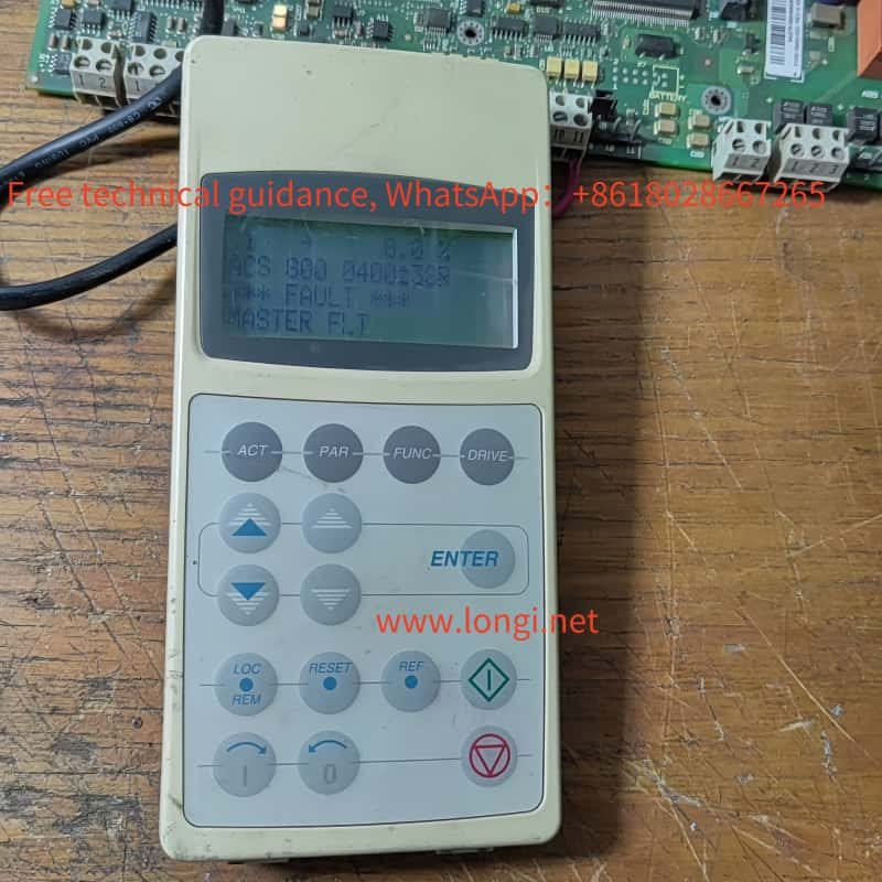
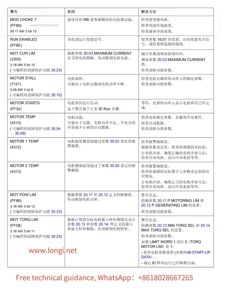
Alarm Message: FF89 – MOD CHOKE T (FF89) 09.11 AW 3 bit 13
Cause:
Overheating of Reactor in Liquid-Cooled R8i Inverter Module The reactor in the liquid-cooled R8i inverter module has exceeded its temperature threshold.
Resolution Steps:
Check the Inverter Fan:
Ensure the inverter fan is operating properly and providing sufficient cooling to the reactor.
Inspect for any blockages or dirt accumulation that may impede airflow.
Inspect Ambient Temperature:
Verify that the ambient temperature surrounding the VFD is within the recommended range.
Ensure there are no heat sources in close proximity that could contribute to overheating.
Examine the Liquid Cooling System:
Thoroughly check the condition of the liquid cooling system, including pipes, pumps, and radiators.
Confirm that the coolant flow rate and temperature are within normal operating parameters.
Inspect for leaks or corrosion that could indicate a need for maintenance or replacement.
Review VFD Operation and Configuration:
Ensure the VFD is not operating under excessive load conditions that could lead to overheating.
Check the VFD’s settings and parameters to verify they are appropriate for the application and load requirements.
Check for Alarms or Warnings in the VFD’s Diagnostic System:
Use the VFD’s diagnostic tools or software (such as DriveWindow) to check for any additional alarms or warnings that may provide further insight into the issue.
Service and Maintenance:
If the above steps do not resolve the issue, consider scheduling preventive maintenance or contacting ABB support for further assistance.
By following these resolution steps, you can effectively diagnose and address the FF89 alarm on your ABB ACS800 VFD, ensuring reliable and efficient operation of your industrial automation system.
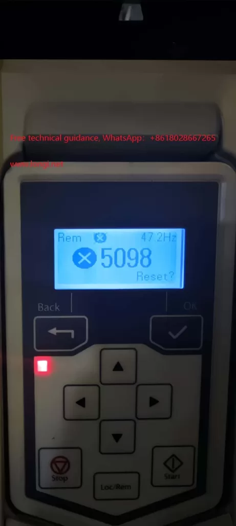
ACS530 VFD 5098 Alarm Fault Analysis and Troubleshooting
When working with ABB’s ACS530 series VFDs (Variable Frequency Drives), encountering specific fault alarms such as the 5098 alarm can be a concern. While the ACS530 series manual may not directly mention this alarm code, by referencing the manual of its similar ACS580 series VFDs, also from ABB, we can gain insight into the 5098 alarm and apply that knowledge to troubleshooting the ACS530 series.
I. Understanding the 5098 Alarm
In the ACS580 series, the 5098 alarm indicates “I/O Communication Lost,” signifying a failure in communication with the standard I/O (Input/Output) devices. This usually occurs when there is an issue with the communication link between the VFD’s I/O terminal board (where analog inputs like AI1 reside) and the main board. Similarly, in the ACS530 series, the 5098 alarm likely indicates a communication issue as well.
II. Possible Causes of the Fault
Power Issues:
The 10V or 24V power supply on the I/O terminal board may be abnormal, leading to unstable or failed communication.
There may be short circuits, open circuits, or poor connections in the power lines.
Hardware Connection Problems:
Connections between the I/O terminal board and the main board may be loose, have cold solder joints, or be corroded.
Terminals may have aged due to prolonged use, resulting in poor contact.
Communication Module Failure:
The VFD’s I/O communication module may be damaged, preventing proper communication with the I/O terminal board.
Software or Configuration Issues:
The VFD’s software configuration may have errors, affecting communication protocols or parameter settings.
Despite similarities in design and software between the ACS530 and ACS580 series, subtle differences in configuration may lead to unexpected alarms in the ACS530 under certain conditions.
III. Fault Troubleshooting Steps
To address the 5098 alarm in the ACS530 VFD, follow these troubleshooting steps:
Check Power Supplies:
Use a multimeter to verify the 10V and 24V power supplies on the I/O terminal board are functioning correctly.
Inspect power lines for completeness, shorts, or open circuits.
Inspect Hardware Connections:
Disconnect all connections related to the I/O terminal board, reconnect them securely, and ensure they are tight.
Examine the connections between the I/O terminal board and the main board for looseness, cold solder joints, or corrosion, and make necessary repairs.
Assess Communication Module:
If possible, test replacing the I/O communication module with an identical one to determine if it’s faulty.
Reset and Restart:
Attempt to reset the VFD to clear the alarm.
If resetting fails, power off the VFD, wait for a while, and then power it back on to eliminate any software-related communication issues.
Contact Technical Support:
If none of the above steps resolve the issue, contact ABB’s technical support team or a professional service provider for further diagnosis and repair.
IV. Conclusion
Despite the ACS530 series VFD manual’s lack of direct mention of the 5098 alarm, referencing similar ACS580 series documentation and contextual analysis enables understanding the likely fault type and appropriate troubleshooting methods. In practice, consider all potential causes
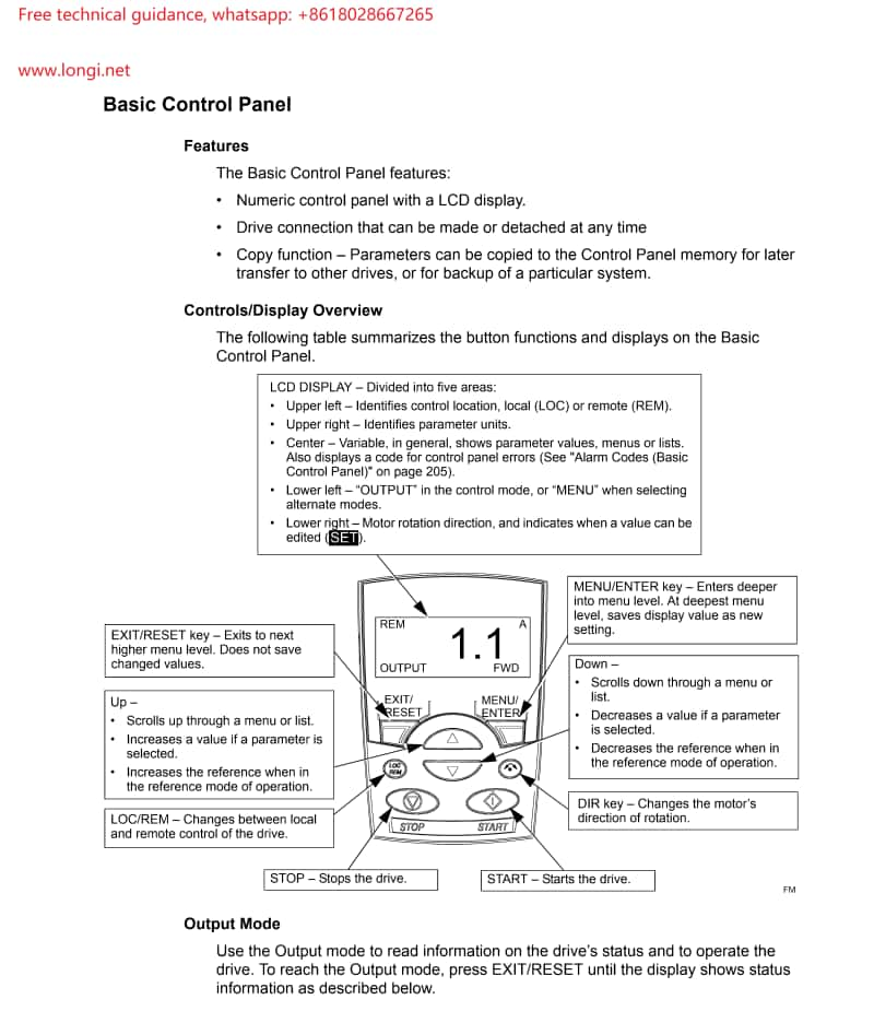
Power On/Off Before powering on, ensure all connections are correct and the surrounding environment meets safety standards. Use the power switch on the operating panel to turn the power on or off.
Mode Switching LOC/REM Button: Used to switch the control mode of the VFD. Press and hold this button for 2 seconds to toggle between Local Control (LOC) and Remote Control (REM) modes. In Remote Control mode, the VFD can be controlled via external terminals or communication interfaces.
Display and Operation Display: The LCD screen on the operating panel displays various status information of the VFD, such as motor speed, current, voltage, etc. Button Operation: Use the Up/Down arrow buttons to navigate through menus and parameters. The MENU/ENTER button is used to enter and exit menus, while the EXIT/RESET button exits to the previous menu level or resets settings.
Parameter Modification Enter the parameter mode, select the parameter group to be modified, adjust the parameter value using the Up/Down arrow buttons, and save the settings with the SAVE button.
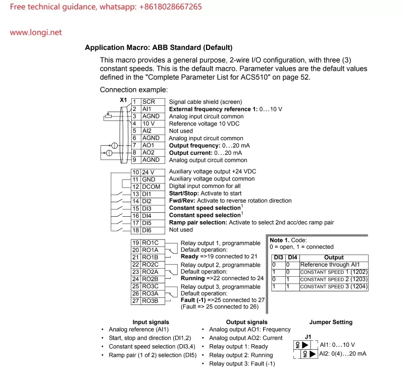
II. VFD Terminal Start-up and Potentiometer Speed Control Wiring Methods
Terminal Start-up Wiring External Start Signal: Typically, connect the external start signal (e.g., a push-button switch) to the DI1 (Digital Input 1) terminal of the VFD and connect the common terminal to DI COM (Digital Input Common). Direction Control: If direction control is required, connect the direction signal to the DI2 terminal. Run Enable: Some applications may require an additional run enable signal, which can be connected to the appropriate DI terminal.
Potentiometer Speed Control Wiring Analog Input Wiring: When using a potentiometer for speed control, connect the output terminal of the potentiometer to the AI1 (Analog Input 1) terminal of the VFD and connect AI COM (Analog Input Common) to the common terminal. Parameter Setting: In parameter group 11, set Reference 1 Select (REF1 SELECT) to AI1 to ensure the VFD receives the speed reference signal from AI1.
III. Parameter Settings
Selecting Standard Macros Enter parameter group 99, find parameter 9902 (APPLIC MACRO), set it to 1, and select the ABB standard macro. This will automatically set a predefined set of parameters suitable for most general applications.
Motor Parameter Settings Input the motor’s rated voltage (9905 MOTOR NOM VOLT), rated current (9906 MOTOR NOM CURR), rated frequency (9907 MOTOR NOM FREQ), rated speed (9908 MOTOR NOM SPEED), and rated power (9909 MOTOR NOM POWER), ensuring these parameters match the data on the motor’s nameplate.
Other Important Parameters Acceleration Time (2202 ACCELER TIME 1): Sets the time required for the motor to accelerate from rest to maximum frequency. Deceleration Time (2203 DECELER TIME 1): Sets the time required for the motor to decelerate from maximum frequency to rest. Maximum Output Frequency (2008 MAXIMUM FREQ): Sets the maximum frequency output of the VFD.
IV. VFD Fault Code Analysis and Resolution Methods
Overcurrent Fault (Code 1: OVERCURRENT) Cause: Motor overload, excessively short acceleration time, motor fault, etc. Solution: Check if the motor is overloaded, increase the acceleration time, inspect motor and cable connections.
DC Overvoltage (Code 2: DC OVERVOLT) Cause: Excessively high input voltage, excessively short deceleration time, improper braking resistor, etc. Solution: Check the input voltage, increase the deceleration time, inspect the braking resistor configuration.
Overtemperature Fault (Code 3: DEV OVERTEMP) Cause: Excessively high ambient temperature, faulty cooling fan, dust accumulation, etc. Solution: Lower the ambient temperature, clean dust, replace faulty fan.
Motor Stall (Code 12: MOTOR STALL) Cause: Motor or load stall, improper motor selection, etc. Solution: Inspect the motor and load, ensure correct motor selection.
Panel Loss (Code 10: PANEL LOSS) Cause: Communication fault between the control panel and the VFD. Solution: Check control panel connections, communication settings, and cables.
Please follow this guide for operation and adjust parameters and wiring according to actual conditions. If any issues arise, please contact us technical support promptly.
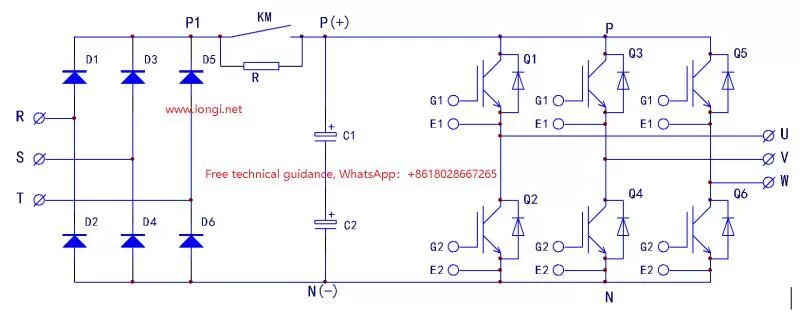
The main circuit of the inverter is a voltage-type, AC-DC energy conversion inverter. Since there is a large-capacity capacitor energy storage circuit between the rectifier and inverter circuits, and the voltage across the capacitor cannot change suddenly, in the initial power-on stage, the capacitor device is equivalent to a “short circuit”, which will form a huge surge charging current, which will cause a large current impact on the rectifier module and cause it to be damaged, and will also cause the air circuit breaker connected to the inverter power supply end to trip due to overcurrent.
The conventional processing method is to connect a current limiting resistor and a charging contactor (relay) in series between the rectifier and the capacitor energy storage circuit. The control of the capacitor charging process is as follows:
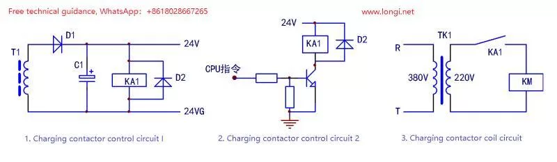
When the inverter is powered on, the charging resistor first limits the current of the capacitor to suppress the maximum charging current. As the charging process extends, the charging voltage gradually builds up on the capacitor. When the voltage amplitude reaches about 80% of 530V, two control processes occur. One is that the switching power supply circuit of the inverter starts to oscillate. The 24V output of the switching power supply directly drives the charging relay, or the relay connects the coil power supply circuit of the charging contactor. The charging contactor (relay) is closed. When the charging current limiting resistor is short-circuited, the inverter enters the standby working state. After a certain voltage is established on the capacitor, its charging current amplitude is greatly reduced, and the closing/switching current of the charging contactor is not too large. After that, the power supply of the energy storage capacitor circuit and the inverter circuit is supplied by the closed contactor contacts, and the charging resistor is short-circuited by the normally open contact of the contactor. The second is that as the charging voltage on the capacitor is established, the switching power supply starts to oscillate, and the CPU detects the voltage amplitude signal sent by the DC circuit voltage detection circuit, determines that the charging process of the energy storage capacitor has been completed, and outputs a charging contactor action instruction. The charging contactor is powered on and closed, and the capacitor charging process ends.
The common main circuit forms of the inverter and the charging contactor control circuit are shown in the figure below:
Figure 1: Common types of inverter main circuits
Figure 2: Control circuit of charging contactor
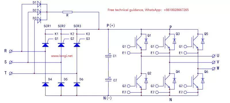
For some inverters and high-power inverters, the rectifier circuit often adopts a three-phase half-controlled bridge circuit, that is, the lower three arms of the three-phase rectifier bridge are rectifier diodes, and the upper three arms use three unidirectional thyristors, using thyristors as “contactless switches” to replace charging contactors. This saves installation space and improves circuit reliability. The circuit form is shown in the figure below:
Figure 3: Control circuit of charging contactor
Although the charging contactor is omitted, the working principle is the same, but the control circuit is different. During the power-on period of the inverter, D1 ∽ D6 is used for rectification, and R is used for current limiting to charge C1 and C2. When the charging process is close to the end, the CPU outputs the opening instruction of the three thyristors SCR1 ∽ SCR3, and the control circuit forces the three thyristors to conduct. The power-on pre-charging circuit composed of D1, D2, D3, and R is used. SCR1 ∽ SCR3 and D4, D5, and D6 form a three-phase rectifier bridge. At this time, the thyristor is in a fully conductive state, which is equivalent to a rectifier diode.
The opening of the thyristor requires two conditions: 1. The positive voltage between the anode and the cathode; 2. A trigger current loop is formed between K and G. The circuit is connected to the three terminals of the AC input power supply to provide unidirectional controlled rectification. During the three positive half-wave voltages of the three-phase AC power, if the trigger current is formed at the same time, the three thyristors can be opened. The first condition has been formed naturally, and the second condition is sufficient to control its opening.
To put it simply, as long as a trigger current (pulse or DC) is provided to the thyristor during the period when the thyristor is subjected to a forward voltage – when the AC voltage passes through zero, the thyristor can be turned on well during the positive half-wave of the AC power and rectify the input AC voltage (just like a diode). The simplest trigger circuit is to introduce a resistor from the anode to the G pole, and during the positive half-wave of the AC power (after the zero point), the trigger current is synchronously introduced to the thyristor to turn on the thyristor. For example, the main circuit form of Dongyuan 300kW inverter is the same as Figure 3, and the trigger circuit is relatively simple:
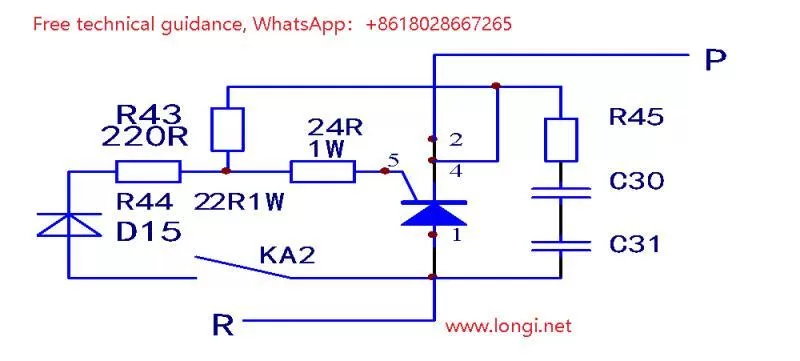
Figure 4: SCR trigger control circuit 1
Figure 4 is one of the thyristor trigger circuits. The other two trigger circuits are the same. The components R45, C30, C31 and other components connected in parallel at the anode and cathode of the two thyristors are peak voltage absorption networks to provide overvoltage protection for the thyristors. The KA2 contact, D15, R44, and 24R form a trigger current path. The function of D15 is to rectify the input voltage half-wave to prevent the thyristors G and K from being subjected to the impact of reverse trigger voltage/current. R44 and 24R are current limiting resistors to limit the peak trigger current and protect the safety of the thyristors. R43 is a noise elimination resistor to increase the reliability of the thyristor operation.
When the CPU issues a thyristor on command, relay KA2 is powered on and closed, a positive half-wave voltage is input, rectified by D15, limited by R44 and 24R, flows into the G pole of the thyristor, and flows out from the K pole, forming a trigger current path, and the thyristor is turned on. The thyristor in the circuit is not in the voltage regulation working area, the conduction angle is the largest, and it is in the “full conduction state”, just like a switch device, only in the two states of conduction and cutoff, without the third state of phase shift (voltage regulation). This is where attention needs to be paid. Therefore, the control circuit is different from the conventional phase shift control circuit and is relatively simple.
A slightly more complex thyristor control circuit, such as the trigger circuit of the Delta 37kW inverter thyristor, is shown in the figure below:
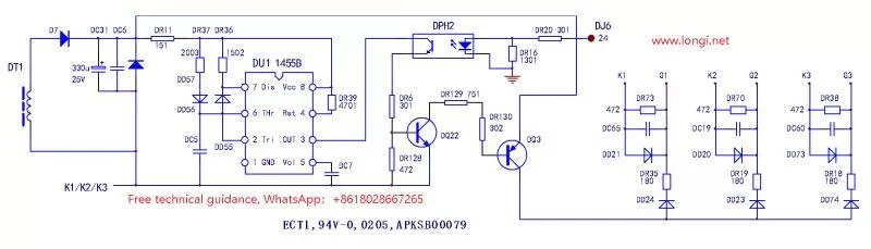
Figure 5: SCR trigger control circuit 2
After rectification and filtering by an independent power supply winding of the switching power supply, it is used as the power supply for the thyristor trigger circuit. The control circuit consists of the NE555 time base circuit, the DPH2, DQ22, DQ3 trigger pulse on/off circuit, and the D and R three-way trigger flow circuit. After the switching power supply works, the NE555 time base circuit is connected to a multi-resonance oscillator and is powered on. Whether the oscillation pulse output from pin 3 is sent to the three trigger circuits of the subsequent stage depends on the command control of the CPU. The command signal of the CPU is introduced to the input side of the photocoupler DPH2 through the 24th pin of the control wiring terminal DJ8. When the transistor on the output side of the optocoupler is turned on, the pulse signal of the NE555 oscillator is sent to the D and R trigger circuit loop of the subsequent stage through the transistors DQ22 and DQ3. After the CPU issues the thyristor opening command, the three devices DPH2, DQ22, and DQ3 are always in the on state, and the trigger pulse is always added to the G and K of the three thyristors. The peak trigger current is about 100mA.
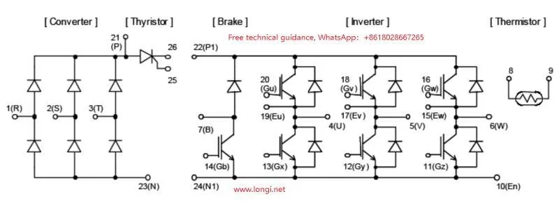
In addition, in the Panasonic and Fuji small power inverter models, another form of main circuit structure is used to complete the initial charging control of the main circuit capacitor. This is the internal circuit structure diagram of the 7MBR35SD120 integrated power module. The circuit is shown in Figure 6:
The difference of the circuit is that a controllable device is added after the three-phase rectifier bridge. A charging resistor must be connected in parallel to the terminals 21 and 26. After a certain charging voltage is established on the main circuit capacitor, a trigger current is input from terminals 25 and 26, then the thyristor is turned on and the inverter enters the standby working state.
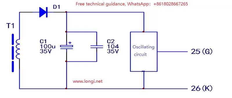
The control circuit is generally powered by an independent 24V winding of the switching transformer to obtain control power with a “floating ground”. The control circuit is mostly an oscillation circuit, which increases the pulse trigger current of the thyristor device. The oscillation circuit is not a conventional phase-shift trigger circuit, but provides high-frequency/density random trigger pulses to put the thyristor in a fully conductive state. The thyristor here, under the action of high-density trigger impulses, is like a switch “turned to the on position”. There is no actual surveying circuit on hand for the trigger circuit of this model, so we can only draw a simple diagram based on the circuit structure for reference.
Figure 6: 7MBR35SD120 integrated power module
Figure 7: thyristor trigger circuit of 7MBR35SD120S module