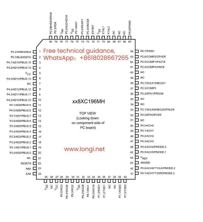
1. Pinout of the 80-pin S87C196MH (MC) microcontroller in SMD package:
2. Introduction to the structure and functions of the S87C196MH (MC) microcontroller:
The controller is a 16-bit microcontroller produced by Intel. It is widely used in inverter products due to its powerful functions and high versatility.
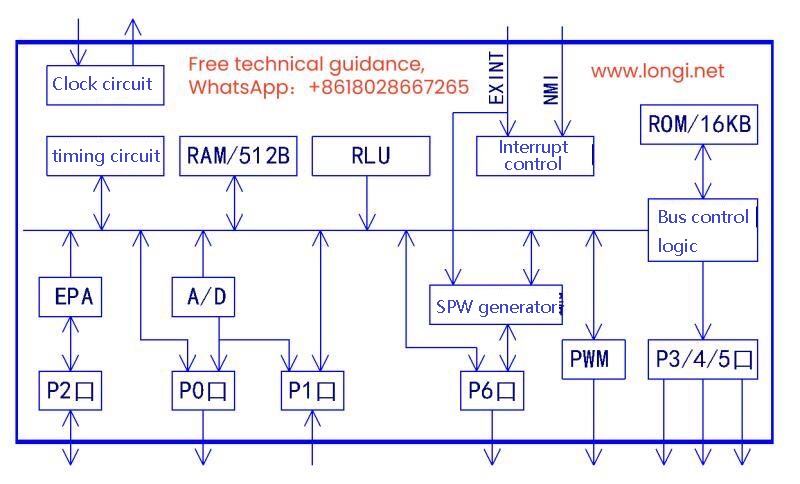
The internal circuit includes arithmetic logic unit (RLU), registers, internal A/D converter, PWM generator, event processing array (EPA), three-phase to complement SPWM output generator, watchdog, clock and interrupt control circuits, etc. The internal structure schematic is as follows:
The S87C196MH (MC) microcontroller uses CHMOS technology, has an operating temperature of -40 º C–85 º C, supports 16KB EPROM, and when the crystal oscillation frequency is 16MHz, it only takes 1.75 μs to complete 16-bit by 16-bit multiplication . It is suitable for the rapidity requirements of the control system. There are 7 I/O ports, and each port pin is multifunctional.
The register array has 512B, which is divided into low 256B and high 256B. The low 256B can be used as 256 accumulators during ALU operation, and the high 256B is used as register RAM. The high 256B can also be switched to 256B with accumulator function through unique window technology. The microcontroller has 13 10-bit/8-bit high-speed A/D converters inside, and the conversion time can be set between 1.39-40.2 μs . The A/D can also be used as a programmable comparator to generate an interrupt when the input crosses a threshold level.
The event processing array (EPA) mainly performs input and output functions. In input mode, the EPA monitors the changes in the input pin signal and records its time value when the event occurs. This process is called capture. In output mode, when the timer matches a stored time value, the output pin is set, cleared or triggered. Both capture and compare events can generate normal service processes or interrupts. There are 4 capture/compare modules and 4 compare modules.
EPA also contains two 16-bit bidirectional timer/counters T1 and T2. T1 can be timed according to an external clock source. In this working mode, EPA can directly process two pulse signals with a 90 ° phase difference output by the position sensor (such as a photoelectric encoder) to monitor the speed and direction of the motor.
External event processing server (PTS). The controller has two types of interrupt systems: programmable interrupt controller and PTS. The programmable interrupt can be set to PTS interrupt service mode. PTS has several micro-instruction coded hardware interrupt service processes, which can work in parallel with the CPU and can complete data block transfer, process multi-channel A/D conversion, control serial communication and other functions.
The S87C196MH (MC) microcontroller has a three-phase complementary SPWM waveform generator built in, which directly outputs six SPWM signals through the P6 port. The driving current can reach 20 mA and the driving frequency can reach 8MHz. Each SPWM signal can be independently programmed and the dead zone interlock time can be set.
3. Application of S87C196MH (MC) in INVT inverter motherboard:
(1) Power supply, clock, reset, etc. Pins that meet the basic working conditions of the microcontroller.
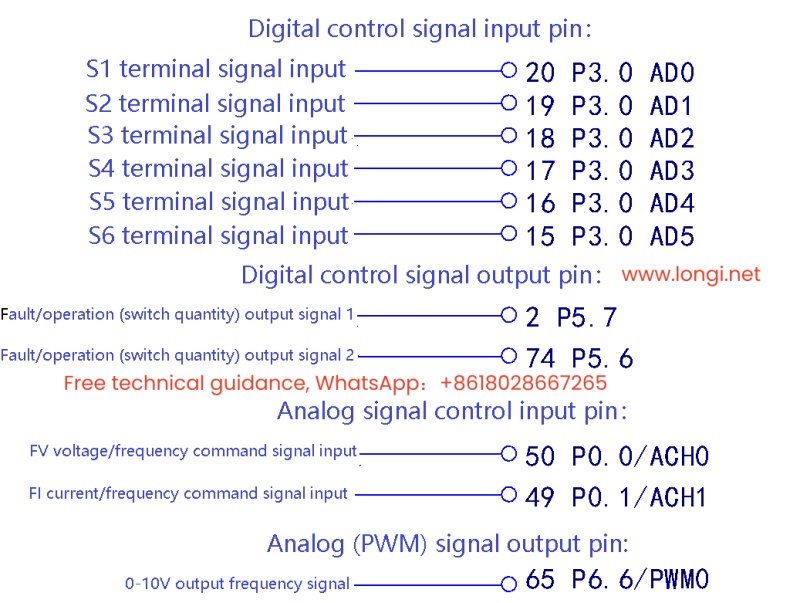
(2) Pins for processing digital and analog signals at the control terminals. The start, stop and speed control of the inverter, as well as the monitoring of the working status, are all carried out through the control terminals. The input and output signals of the control terminals directly enter the microcontroller pins.
The output of the analog signal of the inverter control terminal actually comes from the PWM0 (P6 I/O port) pin of the microcontroller. The actual output is a width-modulated pulse signal, which is converted into an analog voltage signal by the subsequent circuit.
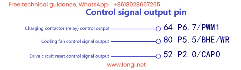
(3)Switching control signal, control of charging contactor (relay control), control of cooling fan and reset control of drive circuit (release its fault lock state).
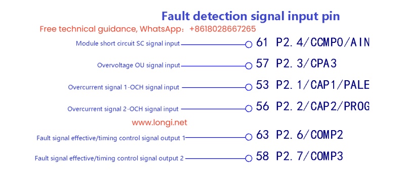
(5)Processing of various detection and protection signals:
(6) Processing of other functional pins
Some pins are connected to ground, +5V, or +5V via a pull-up resistor according to their functions. Some pins are left unused.
The specific functions of each pin of the S87C196MH (MC) microcontroller have been explained in detail above. In troubleshooting, the cause of the fault can also be determined and the fault location can be found based on the level status of the relevant pins.
For example, if the signal input of a certain terminal of the inverter is invalid, measure whether there is a 0-5V voltage change on the corresponding pin of the CPU , and then quickly determine whether it is a terminal input circuit fault or a CPU fault.
The operation control terminal of the frequency converter receives, outputs and processes two types of signals: digital and analog. Analog signals are generally used to input frequency instructions of 0-5V (10V) to determine the output speed of the frequency converter; output analog voltage signals corresponding to the output (given) frequency for external frequency meters to display the operating frequency, etc. The input signals of digital signals are used for the start/stop and fault reset of the frequency converter; the output switch signals are used for external relays and indicator lights to monitor the fault or operating status of the frequency converter, etc.
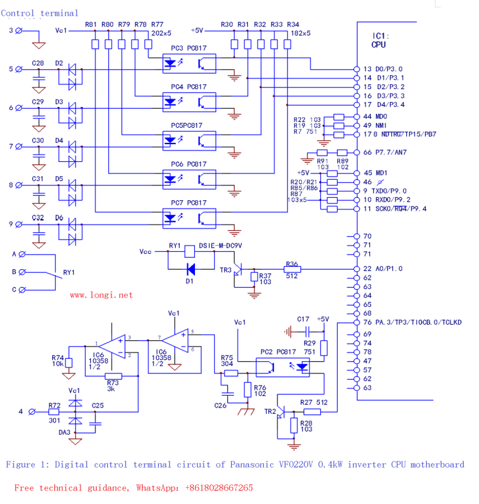
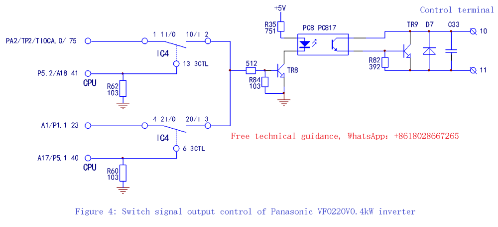
The following figure (Figure 1) is a digital control terminal circuit, 3 is a digital signal common terminal, 5, 6, 7, 8, 9 are digital signal input terminals. When any of the signal input terminals is connected to the common terminal 3, it can form an input path of the optocoupler, thereby transmitting the control signal to the CPU. The benefit of using optocouplers is that in addition to achieving electrical isolation, it also improves the anti-interference performance. The signals of the inverter control terminal, both input and output, are directly from the CPU pins. Pins 13 to 17 of the CPU are the switch control signal input pins. Pin 22 outputs the switch signal, and the signal content (operation, fault, etc.) can generally be set by parameters, also known as the programmable output terminal. The output signal provides a forward base bias current for the control switch tube TR3 through R36. The conduction of TR3 directly drives the RY1 relay, and the switch signal is output from the three terminals A, B, and C for the external indicator light or relay to indicate the working status of the inverter.
The output from the 76th pin of the CPU is a pulse signal representing the output speed, which drives the transistor TR2 through R27, and TR2 drives the optical coupler PC2. The pulse signal output by PC2 is filtered into a smooth DC voltage by R75 and C28, and is added to the subsequent two-stage voltage follower for current amplification, and then outputs a 0-10V (frequency output) analog signal from the control terminal 4. This circuit can actually be regarded as a simple analog/digital conversion circuit. Although the terminal output is an analog voltage, the CPU output is still a digital (pulse) signal.
For digital (switching) signals, at any time, the input and output potentials of the circuit are both in two states: 0 (ground potential of the power supply) and 1 (positive terminal potential of the power supply).
Figure 1: Panasonic VFO 220V 0.4kW inverter CPU motherboard circuit 2: digital control terminal circuit
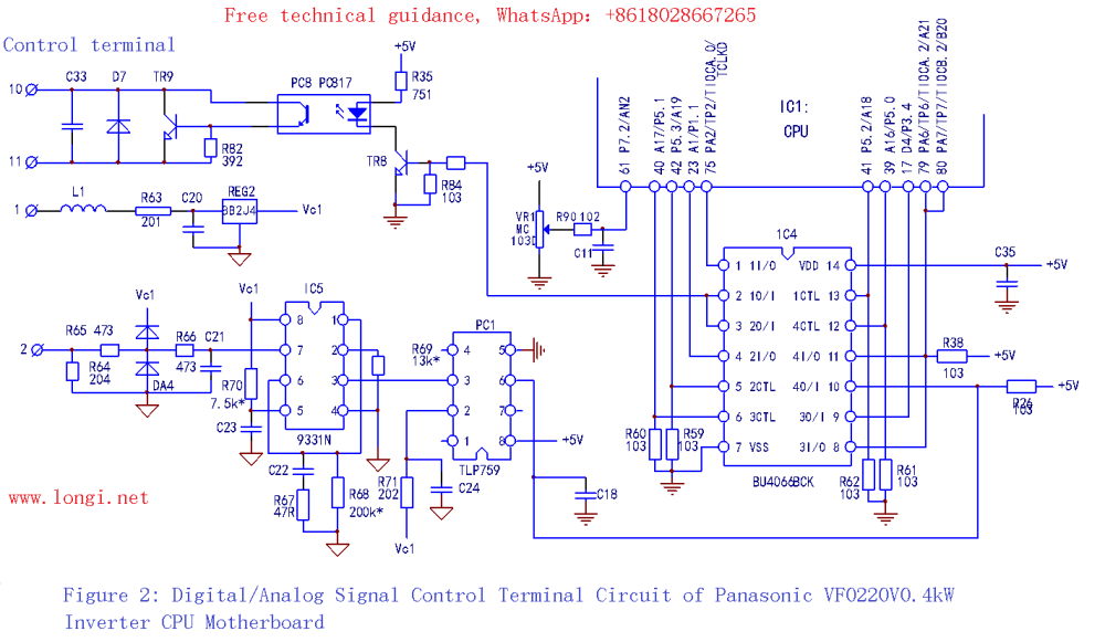
The following figure ( Figure 2 ) is still part of the control terminal circuit. Because the four bidirectional analog switch circuits of IC4 (BU4066BCK) are used for unified input and output processing, the digital/analog circuits are drawn together for ease of reading. IC4 can transmit digital and analog signals. It contains four sets of bidirectional switches. Each set of switches has an independent on/off control terminal CTL. When the terminal is at a low level, the switch is in the off state, and the I/O and O/I are in a high impedance state; when the CTL terminal is at a high level, the switch is in the on state. The purpose of using a bidirectional analog switch is to make the transmission of the signal controlled by the CPU instruction, thereby realizing programmable input and output control. The circuit switches the input of two input signals and switches the output of two digital signals.
Figure 2 Panasonic VFO 220V 0.4kW inverter CPU motherboard circuit 3: digital/analog signal control terminal circuit
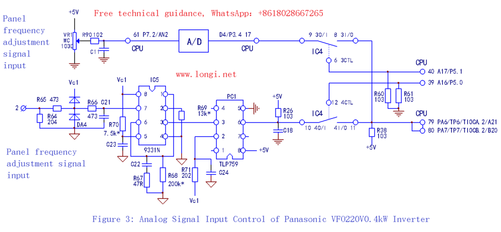
For the switching control of the two input analog signals, in order to facilitate the principle analysis, the analog signal path in the circuit of Figure 2 is redrawn as follows:
Panel frequency command circuit: VR1 is a potentiometer on the operation display panel, which can adjust the inverter output frequency from the operation panel. The adjustment voltage of VR1 is input to the 61st pin of the CPU through the R90 and C11 anti-interference circuits, and after internal A/D conversion, it is output from the 17th pin, through the IC4 bidirectional analog switch, and connected to the 11th pin of IC4, and then input to the 79th and 80th pins of the CPU;
Terminal frequency command circuit: The control terminal 2 inputs the variable voltage signal of the center arm of the external potentiometer, which is first converted by IC5 (93321N) into a U/F signal and then converted into a frequency signal proportional to the input voltage. It is then sent to another set of bidirectional analog switches inside IC4 through the PC1 (TLP759) photocoupler and output from pin 11.
The two frequency command signals are controlled by the level states of the CPU’s 39 and 40 pins, and further controlled by the user’s control intention. The control parameters can be set. When the 40 pin is high and the 39 pin is low, the CPU inputs the frequency command from the operation panel and determines the output frequency accordingly; otherwise, the control terminal is connected to an external potentiometer (or other analog voltage control signal, such as an instrument output signal, etc.) to adjust the output frequency.
Control terminals 10 and 11 are open collectors, and the switch signal output can realize programmable output. The user sets the output content through parameters, or the terminal is connected during operation, or the terminal is connected during failure. Under the control of the CPU’s 41-pin output instruction, when the analog switch 1 and 2 are connected, the photocoupler PC8 is driven by TR8 and turned on, and the terminals 10 and 11 are in a low-resistance state, outputting an operation signal; when the analog switch 3 and 4 are connected by the CPU’s 40-pin output instruction, the terminals 10 and 11 are also in a conducting state, but the output at this time is the inverter fault signal.
Similarly, the content of the output signal depends on the user’s intention – the CPU’s instructions. The two sets of analog switches play the role of a two-throw switch. Different output contents are switched according to the user’s intention.
From the perspective of application maintenance, it is enough to master the pin functions of some IC devices, so as to measure the voltage (level) status of some pins and judge whether the IC is in normal working condition. It is too late and unnecessary to care about what kind of circuit is inside the IC. For example, for the single-chip microcomputer circuit, it is enough to focus on detecting the voltage (level) status of the power supply, reset, crystal oscillator, control signal, and input signal terminals. For digital (including optocoupler) circuits, in general, knowing the pin functions of the device, it is possible to measure and judge the quality of the IC based on the logical relationship between the input and output terminals. As for the analog circuit, half of it is used to process switch signals in the inverter circuit, such as voltage comparators, etc., and it is as convenient to detect and judge as digital circuits. Some analog circuits that process analog signals can be measured based on the obvious changes in dynamic and static voltages, which is not too difficult.
Therefore, as long as you know two points, 1: What type of chip is the IC, digital or analog circuit? 2: The pin function, is the pin an input, output or power supply pin? Then you can implement the measurement. The commonly used IC pin function diagrams of inverters are concentrated in the appendix, so you don’t have to spend a lot of time to consult the relevant manuals.
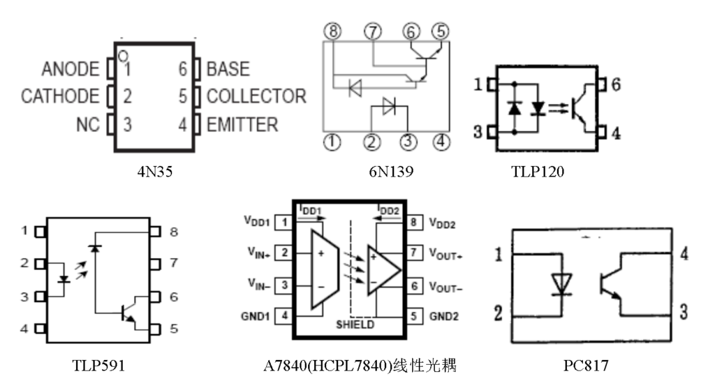
1. CPU (microcontroller) chip and peripheral IC circuit pin function diagram:
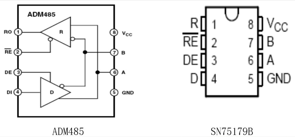
(6) RS485 communication module pin function diagram:
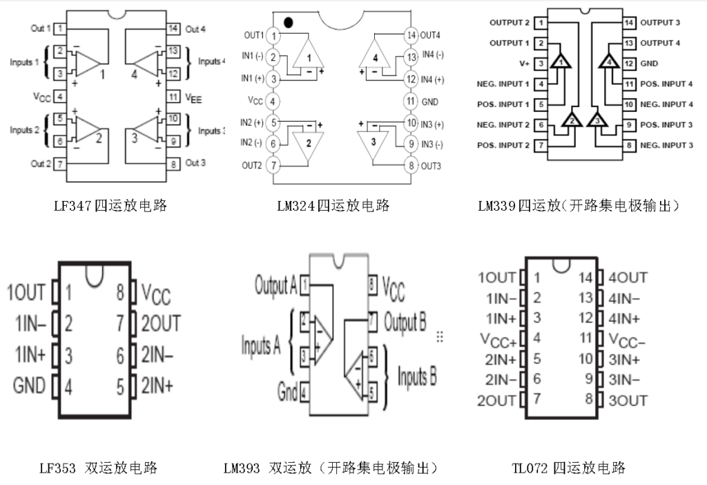
(2)Commonly used operational amplifier pin function diagram:
LF353 dual op amp circuit LM393 dual op amp (open collector output) TL072 quad op amp circuit
Operational amplifiers are mostly used in current and voltage detection circuits to process analog signals and convert them into switch signals – alarm and shutdown protection signals. Open collector output types are mostly used in voltage comparator circuits. Operational amplifiers have good interchangeability. For example, LF347, LM324, and TL072 can all be directly replaced. When the pin arrangement is inconsistent, the terminal wiring can also be replaced.
Open collector output operational amplifiers must be replaced with amplifiers of the same type.
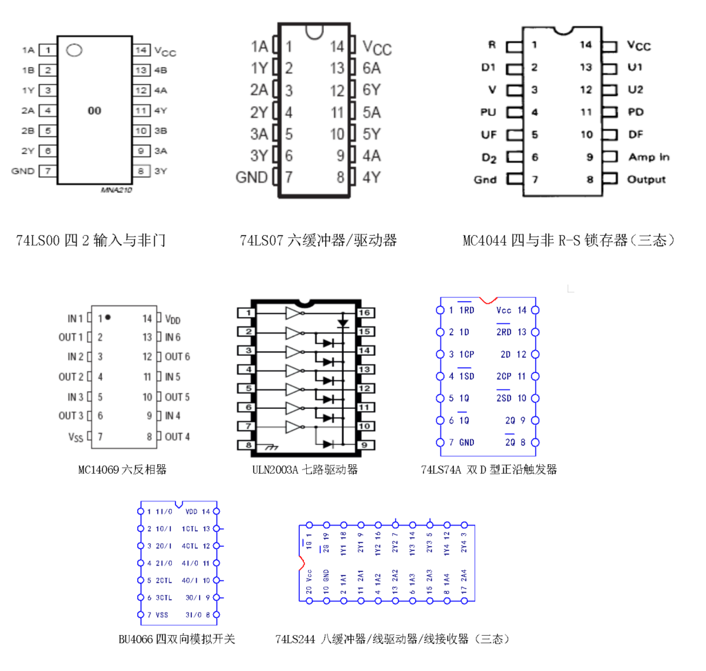
3. Commonly used digital IC circuit pin function diagram:
Digital integrated circuits are also divided into several types according to different materials and manufacturing processes. However, they are mainly TTL (transistor-transistor logic) integrated circuits and CMOS (complementary metal oxide semiconductor logic) integrated circuits. The 74 series TTL circuits and the 4000 series CMOS circuits are the most widely used and have the largest number of applications. TTL circuits consume slightly more power, but have higher operating frequencies and stronger output current capabilities, and the power supply voltage is 5V; CMOS circuit characteristics are the opposite. There is a wider power supply voltage range (3.0-18V ) . Under 5V power supply conditions, the same type of circuits can be interchanged. Under different power supply conditions, if the TTL circuit is damaged, you can consider replacing it with a CMOS circuit.
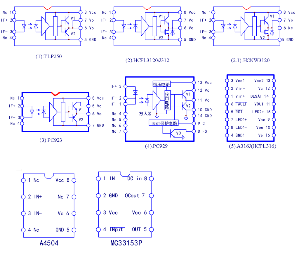
4. Commonly used driver ICs:
TLP250 and HCPL3120 can be directly replaced, and the output pins can be changed to replace PC923. PC923 and PC923 are often used in combination, while A4504 and MC33153 are also used in combination. The combination of the two completes the function of PC929.
5. Commonly used photocouplers:
Optocouplers are used in the control terminal circuit of the inverter, voltage sampling and isolation of the switching power supply, etc. As long as it is a four-wire terminal component, it can often be replaced by PC817. Linear optocouplers cannot be replaced by ordinary optocouplers, and it is best to replace them with original model devices.
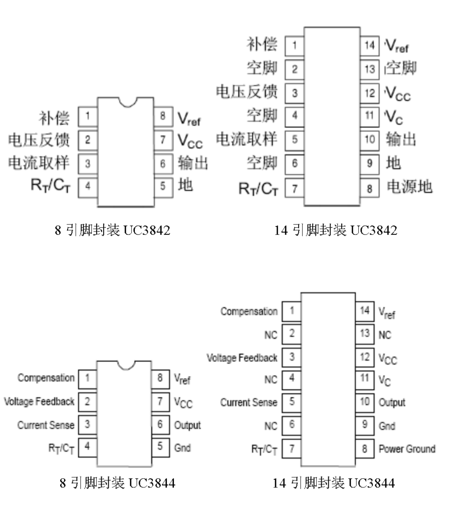
6. Switching power supply oscillation chip:
The pin functions of UC3842 and UC3844 are the same, and both have 8-pin and 14-pin packages. UC3842 and UC3843 can be interchanged; UC3844 and UC4845 can be interchanged.
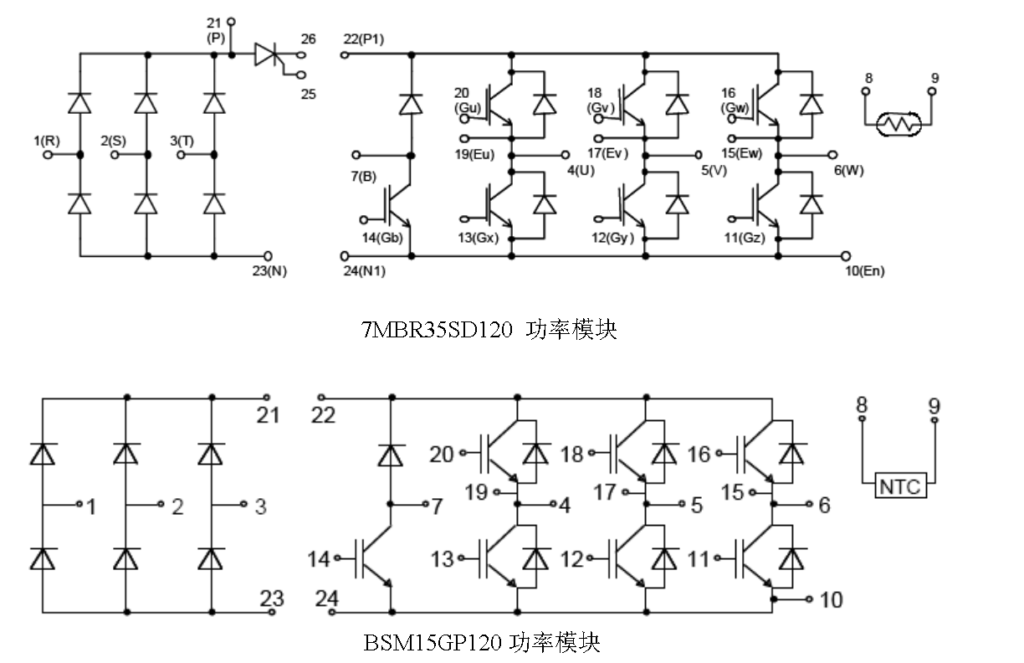
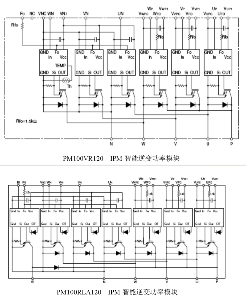
7. Commonly used power (inverter) modules:
The packaging form and size of the power module are consistent, and the rated current value of the replacement module should be equal to or greater than the original damaged module.
Intelligent power modules should be replaced strictly according to the original model.
The structures of the main circuits of all inverters are similar or even identical. The main circuits of Yaskawa inverters and Taiwan Teco inverters are exactly the same. Later I observed that the control panels of the two machines are the same, and the control panel and parameter settings are also similar. It is found that the two machines are similar or even identical from hardware to software, which will bring a lot of convenience to installation, debugging and maintenance. As long as there is a technical data reference at hand, you can debug and repair the two devices.
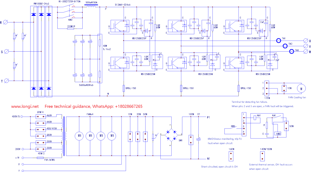
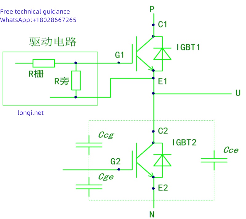
When we open the shells of these two high-power inverters and check the main circuits, the six large rectangular box-shaped objects installed above the inverter modules (in parallel with the modules) will first arouse our interest – the model number MS1250D225P is connected in parallel with the upper arm IGBT tube of each phase, and the model number MS1250D225N is connected in parallel with the lower arm IGBT tube. To use a phrase from the Internet: What on earth is this? What is the purpose of installing it here?
Generally speaking, anything connected in parallel to the IGBT tube, whether it is a capacitor or a resistor-capacitor network, is set up to protect the IGBT tube. That is, when the tube is cut off, the energy formed by the reverse voltage is quickly consumed, providing a reverse current path to protect the IGBT tube from (in fact, it makes it bear less) the impact of reverse voltage. As we all know, whether it is a bipolar or field effect device, there is often a certain amount of surplus in the forward voltage, but the ability to withstand reverse voltage is extremely fragile. Therefore, the things connected in parallel to the IGBT tube can be said to complete this task of consuming reverse voltage.
It should be noted that the internal circuits of MS1250D225P and MS1250D225N were not opened for verification. After the module was damaged, these two devices were often intact, so it was not convenient to disassemble them after they were damaged. The internal circuit in the above figure was drawn based on measurement and speculation, and is only a reference for readers. I have searched a lot of information and searched on the Internet, but I have not found any information about this component. It is obviously easy to mislead to analyze the principle based on the speculation of the circuit. Therefore, the analysis of its principle is temporarily omitted.
However, after connecting such components in parallel to the module, it will bring us new experience in maintenance. See below.
According to the conventional maintenance method, after replacing the damaged module, before conducting the power-on test, we must cut off the P point in the above figure, connect two 25W (or 40W) bulbs in series, and then power on. In this way, if the inverter module circuit or drive circuit is abnormal, causing the two IGBT tubes of the upper and lower arms to short-circuit the DC power supply, the expensive IGBT module will not be damaged due to the current limiting effect of the bulb. Other brands of inverters connect small-capacity capacitors of the picofarad level in parallel at both ends of the tube. After powering on or starting the inverter, as long as the U, V, and W output terminals are unloaded, the bulb will not light up. But the performance of Yaskawa inverters in maintenance is different. Connect a bulb in series at point P, power on, and the bulb does not light up. It is correct, I breathed a sigh of relief; press the operation panel to start the inverter, and the bulb becomes bright! It is broken, the output module has a short circuit! This is my first judgment. Check the module and drive circuit during power outage, and there is no abnormality. Looking back at the circuit structure, after removing the MS1250D225P and MS1250D225N, the light bulb did not light up after starting the inverter. The three-phase voltage of the no-load output was normal. These two components and the external 10 Ω 80W resistor provided a current path of about 100 mA, making the 25W bulb bright. Sacrificing tens of watts of power consumption in exchange for higher safety of the IGBT tube is the characteristic of the module protection circuit of the Yaskawa inverter.
After the inverter is started without load, due to the relationship between components such as MS1250D225P and MS1250D225N, the inverter circuit itself forms a certain circuit path, which is not caused by the inverter module failure. This machine is a special case. The existence of a circuit path does not necessarily mean that the module is damaged. Observe which components provide the current path? When fresh experience solidifies into a fixed mindset, misjudgment of faults is inevitable.
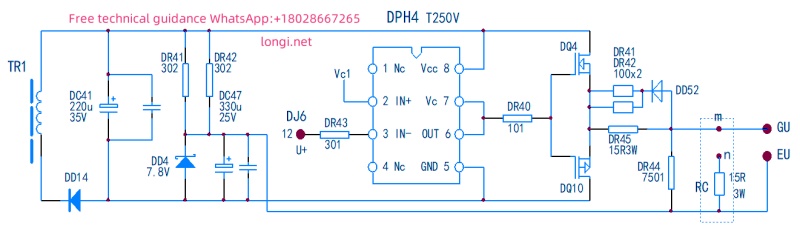
The control power of the whole machine is obtained from a multi-tap transformer at the bottom of the figure. The short-circuit wires of sockets 3CN and 4CN are different, and the level of input voltage can be adjusted to ensure the accuracy of the secondary winding AC220V voltage. The cooling fan uses an AC220V power supply, which is filtered and used as the input of the switching power supply. When repairing the driver board alone, the terminals 2 and 3 of the fan; 3 and 4 of the contactor terminals; 14CN, 15CN, and 16CN must be short-circuited, and fault signals such as undervoltage (FU/LU), overheating (OH), and fan failure (FAN) must be manually eliminated, so that the CPU can output six pulse signals, which is convenient for checking the drive circuit.
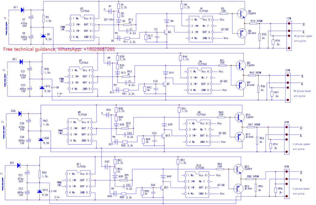
2. Drive/protection circuit of “616G3-55kW Yaskawa inverter”
The types of drive circuits are similar. The most common ones we see are drive detection circuit (protection circuit) is also integrated. Although you can find circuit information about A3316J, etc., and you can see the internal unit block circuit diagram and the introduction of the circuit principle, you always feel a little confused about the specific composition of its protection circuit – the protection circuit inside the IC is indeed invisible and intangible. It happens that this circuit is a detection and protection circuits composed of ICs such as PC929 and A316J, in which the module fault circuit composed of discrete components, which makes it easier to understand the detection and protection action process. Slightly redrawing the pulse and protection circuit in the above figure, you can see how the IGBT tube voltage drop detection circuit implements the protection action on the module:
Circuit principle: The PWM pulse signal from the CPU pin is isolated and amplified by the U2 optocoupler and then sent to the module protection circuit. Under normal conditions, this pulse signal is amplified by the push-pull power amplifier circuit of Q2 and Q3 to directly drive the IGBT module. It is generally believed that the IGBT module is a voltage-type drive module, which is biased. The input gate-emitter junction capacitance of the IGBT tube just needs a transient large inrush current! This is why Q2 and Q3 are used for power amplification. The introduction resistor of the drive signal is also a 5 Ω 8W power resistor. In this sense, in essence, the IGBT module is still a current-type drive device. This is the author’s opinion, is it correct? When the current output capacity of the drive circuit is insufficient, the three-phase output current will be intermittent, the motor will vibrate, and a rumbling sound will be emitted. The principle of the pulse processing circuit can be found in other figures. The focus here is on how the protection circuit works.
When the inverter does not receive the start signal, the output pins 7 and 8 of U2 are cut-off negative voltages. If the 0V power line is used as the reference point, the voltage of pins 7 and 8 is about -9.5V (ignoring the saturation voltage drop of the internal tube). This negative voltage is introduced to the base of Q2 and Q3 through R13 and R3. Q2 is cut off due to reverse bias, Q3 is turned on due to positive bias, and the gate bias of the IGBT module is negative and is in the cut-off state. Resistors R1 and R2 divide +15V and negative -9.5V to obtain a 3V level. D9 is a voltage regulator with a breakdown voltage value of 9V. The voltage division value of R1 and R2 is not enough to cause it to break down, so Q3 has no bias current and is in the cut-off state. There is no input current to the photocoupler U1, so no fault signals such as GF (grounding) and OC (overload, short circuit) are returned to the CPU. When the CPU sends a drive pulse, the 7th and 8th pins of U2 become positive pulse voltages with a peak value of 15V, and the positive pole of D1 rises to +15V at this time. At this time,two situations occur: In one case, the module is good, and the IGBT tube is quickly turned on under the drive of the positive excitation pulse. It can be considered that the P and E points are short-circuited instantly. The negative terminal potential of D1 is instantly pulled to 0V, and the negative terminal potential of D2 is also pulled to below 1V. Because it does not reach the breakdown value of D2, Q3 still has no base bias current and is cut off; In another case, the module has caused the operating current to be too large due to abnormal load, or the IGBT tube is not turned on well due to the poor driving circuit itself such as Q3. The negative terminal of D1 is high potential and is cut off, and +15V causes D2 to break down through R1, Q3 is biased and turned on, and the positive pulse voltage of the base of Q2 is pulled to zero level, and the IGBT module loses the pulse and is cut off. At the same time, the conduction of Q3 generates the input current of U1, and U1 sends the module fault signal to the CPU. It can be seen that the protection circuit of this circuit first cuts off the driving pulse of the IGBT tube and sends out the module fault signal at the same time. The protection is timely and fast.
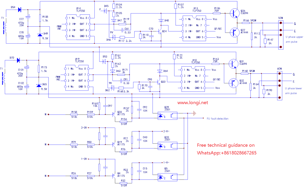
3. Drive/FU circuit of 616G3-55kW Yaskawa inverter
The protection circuit of the drive circuit implements protection actions and sends OC signals according to the tube voltage drop of the IGBT tube during the sending of the excitation pulse. According to the information, the on-state voltage drop of the IGBT module is about 3V under normal (rated current) conditions. When the tube voltage drop reaches 7V or more, it means that the current flowing through the IGBT module has exceeded 180% to 200% of Ie. At this time, the protection action is of course the faster the better. The purpose of setting up this protection circuit is to make up for the slow protection action of the subsequent current detection circuit such as the current transformer. The current detection circuit inevitably uses a large capacity filter capacitor, which makes the circuit have a certain time constant and slow response. The tube voltage drop detection circuit of the IGBT can be called a fast protection action circuit because of its rapid response, just like a fast action unit, which is used to deal with emergency events. The treatment of slight overcurrent and current limiting regulation is still implemented by the current detection circuit of the current transformer circuit.
The drive circuit is also equipped with a fuse detection circuit. In general, a fast-blow fuse is connected in series at the P end of the DC circuit to implement module protection. However, this machine circuit has a fuse connected in series at each phase output module. The inverters produced by each manufacturer generally have the following trends: early products are inevitably crude, old and heavy, and their user control functions are not perfect, but there is a large margin in their production and selection of materials; they are conservative in protection performance, but they do not hesitate to add components that seem redundant now to ensure the reliability of the protection circuit. The early products of Yaskawa inverters were no exception. With the advancement of product technology and the fierce market competition, the functions of inverters have been improved, while the costs have been reduced, and there is even a suspicion of cutting corners. The operating reliability of inverters has also been compromised, and domestic inverters should take this as a warning.
The detection circuit of the three-way fuse blown is to compare the 0V line of the lower three-arm drive power supply with the N line of the main DC circuit to determine whether the fuse is normal. Under normal conditions, the 0V line and the N line of the drive power supply are connected through the fuse and are of equal potential. That is, the E pole of the lower three-arm IGBT tube is connected to the N line of the main DC circuit. Therefore, the base bias of the transistors Q4, Q19, and Q28 is zero. All three tubes are cut off. When the fuse of any phase output module is disconnected, the N line and the 0V line of the phase drive power supply produce a huge potential difference, and the transistor is turned on by positive bias. The three optical couplers Q5, Q20, and Q29 are connected into an OR gate circuit. The input signal of any optical coupler will be transmitted to the same output point, and the fuse signal of the fast insurance will be transmitted to the CPU, so that the CPU reports the FU (fuse) broken signal and refuses to accept the start signal.
There is also an interesting problem of the order of fault signal alarm of Yaskawa inverter. For example, when the power is on, a warning of the fault code is given for overheating, undervoltage, overcurrent, fan failure, fuse failure, etc., and the startup operation is refused; during the startup, the module fault detected by the module protection circuit is warned with the GF (ground fault) code. When the module fault is detected during operation, the OC (operating overcurrent, load short circuit, etc.) fault code signal is reported. The same signal output by the IGBT tube voltage drop detection circuit is output at different times (one is during the startup process, and the other is during the operation process), but the inverter reports two different fault codes (GF: ground fault; OC: overload or short circuit fault). Similarly, in the current and voltage detection circuits, the same means are sometimes used. The overcurrent or overvoltage signal reported by the same protection circuit may report different fault codes or take different treatment measures due to the different working states of the inverter (starting or running). All this depends on the ideas of the software designer. The control ideas of each manufacturer’s inverter must be similar. Pay attention to the relevant characteristics of the inverter fault alarm to facilitate efficient diagnosis of the fault.
When analyzing the protection circuit, you need to look at the main circuit and the drive (protection) circuit in two or three parts. Many drawings are broken down into individual unit circuits. Readers must strengthen their ability to read drawings in a comprehensive and coherent manner. This is a piece of advice I give you.
CPU, also known as central processing unit, is generally composed of arithmetic unit, controller, internal memory, input/output device, interface circuit and bus. However, with the advancement and update of technology, its functions and structure are constantly expanding – the original CPU peripheral circuit is also integrated into the device. When its hardware equipment is expanded to a certain scale, so that it can independently complete a more complex control function, this device is called a microprocessor. In the microprocessor family, in order to be suitable for a certain application field, the hardware structure is different from the general microprocessor (such as 80C51) – there is a certain uniqueness. For example, the microprocessor often used in the inverter referred to in this article has a six-way PWM wave output function and can realize specific control functions. It is also called a microcontroller, alias: single-chip microcomputer. Because people in the industry generally refer to the circuit board of the inverter single-chip microcomputer as the CPU motherboard, from the perspective of convention and concise definition, this book also calls the microcontroller (single-chip microcomputer) CPU.
The microcontroller used for inverter control, also known as “high-performance microcontroller”, should be a dedicated control chip developed specifically. It should have at least six PWM wave forming and output circuits and ports to output the six inverter pulses required by the drive circuit; it should have an A/D conversion circuit, and some should also have a D/A conversion circuit to adapt to the processing of analog input and output quantities; it should have high-speed pulse signal input and output ports and serial port sending and receiving pins to process various digital signals and communication instructions; it should contain program memory and data memory to store programs, original data and rewritable data; of course, it should also have port drivers, various buffers and other circuits, which will not be repeated here.
What goes in and out of each CPU pin is nothing more than some “signal flows”. Some only go in but not out, and go but not return, such as the switch signal input by the control terminal; some only go out but not in, and go but not return, such as the relay signal output by the CPU on the control terminal; some go in and out, such as the signal transmitted between the CPU and the memory, and the operation display panel. This type of signal is bidirectional. All signals can be divided into two categories based on their nature: digital and analog. Voltage detection signals and speed control command signals are often analog, while the start and stop signals of the inverter and keyboard input signals are digital (switch quantity). Some analog signals are processed by the CPU external circuit, such as A/D conversion, before being sent to the CPU. Some directly enter the CPU pins and are processed by the internal A/D circuit. The different CPU hardware function circuits used will inevitably lead to different external circuits.
The integration of microcontrollers is high enough. It is impossible to integrate all the circuit elements required for operation without limit. It needs the active cooperation of external circuits to work. There are three working conditions that are necessary for microcontrollers, the so-called three elements of CPU operation: +5V power supply, working clock, and reset signal. The generation of working clock is generated by the oscillation circuit composed of the internal circuit of the microcontroller and the crystal oscillator element connected to the pin; the reset signal is generated by the external reset circuit when the power is on. A low-level (or high-level) pulse is sent to the reset pin of the microcontroller, and the internal circuit controls the program reset and enters the standby state. The program memory and data memory (referred to as memory) inside the microcontroller have limited capacity and use. External memory-electrically erasable memory is often required to complete some data storage tasks (especially user program storage tasks), which should constitute the four elements of the normal operation of the microcontroller. In order to accept the user’s instructions or inform the user of the working status of the inverter, the microcontroller needs a human-machine interface-operation display panel, communicate with the user, and normal communication with the operation display panel becomes the five elements of the microcontroller’s operation. In addition, the quality of the external circuits of each pin of the microcontroller will affect the operation of the microcontroller. Since then, seven or eight or even dozens of elements of the microcontroller’s operation have appeared. In fact, in my opinion, from the perspective of the microcontroller (or microprocessor, CPU) itself, three elements are necessary for the work. Without them, the microcontroller cannot meet the most basic working conditions. If the microcontroller does not work due to other reasons, it is the external circuit, not the microcontroller itself that is not working, right?
The external circuit and external framework of the microcontroller have been built, but a “body” alone cannot work. It also needs a “soul” to command the operation of the body – the software control program. The program capacity of the inverter is large, generally up to thousands of lines. The control function of the microcontroller is concentrated on two points. One is the control of the output PWM wave. In this regard, there is a clear difference between high-quality and low-quality inverters. Some PWM waves are very optimized, while others are a bit bad – the output torque is small, the operating noise is large, and the carrier interference is also large; the other is the state detection and protection of the inverter module. This task is completed in conjunction with the external circuit, and it is also the focus of the inverter circuit.
Microcontroller – single-chip computer technology has become an important technical branch of automation control technology. I hope that friends can master more relevant knowledge themselves. I will not go into details here.
The failure rate of the CPU motherboard is relatively low, accounting for about 20% of the total failure rate. Failures mostly occur in the fault detection circuit and the control terminal circuit. The inspection and maintenance of the fault detection circuit has become an important inspection content of the CPU motherboard. When the fault detection circuit (subsequent circuits for voltage and current detection, temperature detection circuit) itself is damaged, it is a bit like “falsely reporting military intelligence” and deliberately making trouble. The main circuit is obviously good, but it reports an “output short circuit” fault or an output phase failure fault. The fan is obviously good, but it reports an overheating fault, etc., which prevents the inverter from being put into normal operation. The fault of the control terminal is mostly caused by the user mistakenly connecting to a high voltage, which burns the terminal power supply 24V, the terminal input circuit is open-circuited and damaged, and the input side circuit of the photocoupler is damaged.
The damage rate of the CPU chip itself is less than 2%. Due to the technical blockade involved, the internal program is not easy to crack. General maintenance personnel do not have the relevant conditions to repair the chip. They can only purchase original manufacturer parts or replace the CPU motherboard, the so-called “board-level repair”. However, for partial damage to the CPU chip, workarounds can be used to try to repair it.
2. Principle analysis and maintenance of the basic circuit of CPU:
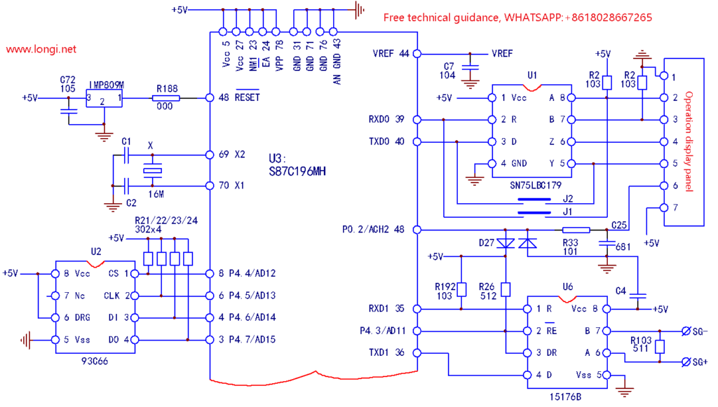
Figure 1. One of the CPU mainboard circuits of INVT inverter G9/P9: Basic circuit of CPU
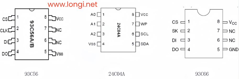
The inverter CPU motherboard circuit, which is the basic circuit for CPU operation, is composed of power supply, crystal oscillator circuit, reset circuit, external memory circuit and operation panel display circuit. The reset circuit is composed of special three-terminal reset components IMP809M and R188. It provides a low-level pulse to the 48th pin of the CPU at the moment of power-on, just like shouting the slogan “Everyone take your place”, realizing system reset and starting the program to run. The 3rd, 4th, 6th and 8th pins are connected to the U2 (93C66) memory. The user control program has been stored inside when leaving the factory. During the debugging and use process, the user needs to modify certain parameters at any time to meet the control requirements. The modified parameter values are stored by U2. The four pins connecting the CPU and the memory are all connected to +5V by pull-up resistors.
The general model of the inverter, the operation display panel, has been used as an independent device to communicate with the CPU. It accepts user instructions and transmits relevant monitoring data. The operation display panel contains CPU, decoding driver, LED display and other circuits, and can perform two-way data transmission with the CPU. Between the operation display panel and the CPU, the RS442/RS485 transceiver realizes communication transfer. The user operation signal is input from the A and B differential input terminals and sent to the CPU from the R receiver output terminal; the data signal output by the CPU enters from the D transmitter input terminal and enters the operation display panel from the Y and Z driver output terminals.
In order to adapt to the new control requirements, the control terminal of the inverter is also equipped with an RS485 communication port. In the figure, U6 (15176B) is an RS485 transceiver. D is the driver input terminal, connected to the CPU’s TXD1 serial port sending pin; R is the receiver output terminal, connected to the CPU’s RXD1 serial port receiving pin; A and B are the receiver input and driver output terminals; DE and DR are the driver and receiver enable signal terminals. The working status of the driver and receiver is controlled by the level signals of these two pins.
CPU basic circuit inspection and maintenance:
The failure rate of the CPU (single-chip microcomputer) itself is extremely low. Except for abnormal situations such as damage caused by lightning strikes introduced by the inverter, electrical failures are rare. The CPU is damaged because it contains running programs. For the sake of technical confidentiality, the manufacturer has taken some confidentiality measures to the greatest extent possible. It is difficult to decrypt the program and re-copy the chip. General maintenance personnel do not have such technical means. Does this also involve the issue of intellectual property rights? Therefore, after damage, it is necessary to purchase a chip with the program copied from the manufacturer, or replace it from a circuit board of the same model, or simply replace it with a CPU motherboard.
The inspection of the CPU basic circuit mainly includes the inspection of its three working elements and other working conditions, and fault repair.
The failure of the CPU basic circuit (three-element circuit) is typically characterized by: after power-on and when the power supply is normal, the operation panel has no display, or displays a fixed character, the inverter has no initialization process, and all operations on the operation display panel fail, similar to the phenomenon that a computer cannot be turned on and “freezes”.
The nature of the fault: A. At least one of the three elements of CPU work is missing, the CPU cannot complete the initialization operation, and the program is “stuck”; B. The CPU detects the existence of a dangerous fault signal during the self-test process and is in a fault lock state. All operations are rejected. This is a “CPU motherboard pseudo-fault” phenomenon. After checking and eliminating the cause of the fault, the CPU “strike” phenomenon will disappear immediately; C. The CPU chip is damaged due to lightning strike or abnormal power supply.
Note: If the program is “stuck”, be sure to eliminate the “CPU mainboard pseudo-fault” first, and then inspect the three elements of the CPU and other circuits. Focus on inspecting the OC fault alarm circuit, see the relevant content of Chapters 4 and 5 for details.
To determine whether the CPU is working or the three-element circuits are normal, you can first make a rough judgment:
(1).When the inverter is powered on, listen carefully to see if there is a “click” sound from the charging relay or contactor. If there is, it means that the three-element circuits are normal and the CPU is working normally. The inverter is in a fault lock state;
(2)Observe the operation display panel. Generally, there is a “power-on character” that flashes and finally stabilizes to a certain character. This process indicates that the CPU has also entered the working state.
(3)If you know the power-on self-test process of the inverter and the potential status of each pin, you can detect the voltage changes and level status of the relevant pins to determine whether the CPU is in operation. Use the key signal input of the operation display panel and the voltage changes of the key points of the detection circuit to determine whether the CPU is in working state. If you press the reset button on the panel, the inverter status signal output relay may make a “click” opening and breaking sound, and at the same time, the reset signal input pin of the drive circuit has a corresponding level change. This means that the CPU can accept the reset signal input and can output the fault reset signal to the drive circuit. This means that the CPU is working normally.
(4)If it is determined that the CPU is not operating normally, the basic working circuit of the CPU can be checked.
Fault inspection of the three-element circuit:
A、 Check the +5V power supply circuit. Check the CPU’s VDD, VSS, Vcc, GND and other power pins to confirm that the power supply is normal. The +5V power supply circuit is often connected to a filter capacitor with a large capacity of thousands of microfarads. When its capacity drops seriously, the CPU program will run disorderly and easily enter a program “dead loop”;
B、Check the reset circuit. The reset circuit provides a pulse voltage for the reset pin of the CPU during the power-on period. The duration of the pulse voltage is μs . Therefore, if a low pulse is required for reset, the static voltage of the CPU reset pin should be +5V. If a high level pulse is required for reset, the static voltage of the CPU reset pin should be 0V low level. Detection methods for the reset circuit:
a. According to the CPU reset pin’s requirement for high or low pulse voltage, measure whether its static potential is normal. If the static voltage is abnormal, check the CPU external reset circuit. You can disconnect the CPU pin to determine whether the abnormal reset pin voltage is a reset circuit failure or the CPU reset pin’s internal circuit is damaged.
b. If the static voltage is normal, you can use the artificial forced reset method to determine whether the CPU can work normally. The method is: if the static voltage of the CPU reset pin is +5V, use a metal wire to quickly short the reset pin and the power supply ground to artificially form a low-level signal input; if the static voltage of the reset pin is 0V, use a wire to quickly short the reset pin and the power supply +5V to artificially form a high-level signal input.
c. After forced reset, if the CPU can work normally, as shown by changes in the content of the operation display panel and the ability to modify parameters, it indicates that the external reset circuit is faulty and the damaged components must be replaced. For dedicated three-wire reset components, if there are no original components to replace, the RC component circuit can be connected for emergency repair;
d. If forced reset is invalid, the crystal oscillator circuit should be further checked.
3. Check the crystal oscillator circuit. The crystal oscillator circuit has few external components, usually only two capacitors and a crystal oscillator. Common circuit faults include the following:
a. Because the crystal oscillator contains quartz crystal, it is easy to break and fail after severe vibration;
b. If the crystal oscillator or capacitor leaks electricity, the signal transmission loss will increase, causing the oscillation to stop;
c. The internal oscillation circuit of the CPU is damaged and the CPU needs to be replaced.
Measurement method: a. The oscillation pulse is a rectangular square wave, and its pin voltage is about the middle value of 0V and +5V. The voltage values of the two pins are slightly different, about 0.3V. Among them, the X2 pin is 2V, and the X1 pin is 2.3V. Please use the voltage range of the digital multimeter when measuring. If you use a pointer meter, due to the low internal resistance, it may cause oscillation to stop, making the measurement result inaccurate; b. If the crystal oscillator leaks slightly or the performance deteriorates, when the crystal oscillator pin is lightly ironed with an electric soldering iron, the CPU motherboard resumes normal operation. It may be that the crystal oscillator is inefficient and the crystal oscillator should be replaced; c. If the crystal oscillator is suspected to be bad, it is best to replace it with a good crystal oscillator for testing. When removing the crystal oscillator for inspection, you can shake the crystal oscillator and carefully observe whether there is a slight clattering sound inside it. If there is, it means that the crystal oscillator is damaged by vibration. Measure the resistance value of the two pins, which should be infinite. If there is a resistance value, it means leakage. If there is a capacitance meter to measure the two pins, a good crystal oscillator has a PF-level capacitance, and its capacitance value decreases with the increase of the nominal frequency. e. There is another rare situation of defective crystal oscillator. Due to structural deformation or mechanical aging, the circuit oscillation frequency is lower than the nominal frequency value, and the frequency of CPU clock pulse is reduced. First, the system operation slows down. Second, due to the change of time reference value, the CPU sampling of input current and voltage signals will have errors, and the display values of running current and output frequency will also have corresponding deviations. In severe cases, the CPU may stop by mistake. The occurrence of this fault is manifested as a difficult fault.
Check the fault of CPU external memory. The inverter can be operated and the parameters can be modified, but after power failure, the modified parameter value cannot be stored, indicating that the machine has an external memory fault. Check the power supply of CPU external memory and the status of the connection line with CPU. Because the “pulse stream signal” is transmitted between CPU and external memory, it is difficult to judge whether it works well or not by the voltage of its pins. You can remove a good memory from the same model circuit board and replace it for testing. Note: If a new blank memory chip is used, the machine will not work. The user control parameters are already stored in the memory when it leaves the factory. If conditions permit, the original storage content can be copied to the new chip. Or purchase the memory chip from the manufacturer and replace it.
Inspection and maintenance of the operation display panel. 1. The buttons and speed regulating potentiometers on the operation display panel are wearing parts. Due to dust and humidity at the work site, they may cause poor contact, unstable output frequency or failure to write parameters. They can be replaced and repaired. 2. The LED display strokes are incomplete. Vibration causes internal drive circuit pins to be poorly soldered, copper foil strips to break, etc., which can be repaired by welding. 3. The power supply is normal, but there is no display, or a fixed character is displayed. You can replace the operation panel with the same model for testing. If the operation display panel is faulty, you can purchase a complete replacement from the manufacturer. 4. If replacing the operation display panel is invalid, check the data communication module between the CPU and the operation display panel – RS442/RS485 transceiver and other circuits.
[ Failure Example 1 ] :
A 7.5kW INVT inverter could not hear the sound of the charging relay closing when powered on, and all control operations failed. The voltage of the CPU reset control pin 48 was measured to be 2.3V, which should be 5V under normal circumstances. It was determined that the three-wire reset element IMP809M was defective. After replacement, the fault was eliminated.
[ Failure Example 2 ] :
A Fuji 5000G9S 11kW inverter had a fixed character displayed on the operation panel and could not be operated. The “program stuck” phenomenon occurred and was determined to be a CPU mainboard failure. The static voltage of the CPU reset control pin was measured after powering on and was normal. The manual forced reset method was ineffective. The fault disappeared when the crystal oscillator soldering pin was heated with a soldering iron. After replacing a high-quality crystal oscillator component and two ceramic capacitors, the fault was eliminated.
[ Failure Example 3 ] :
A Fuji 5000G9S 47kW inverter, the operation panel displays a fixed character, cannot be operated, and the “program stuck” phenomenon occurs, which is judged to be a CPU mainboard failure. After starting the machine for inspection, power on, and measuring the CPU power supply, it is normal, but the CPU chip is hot and has an abnormal temperature rise. It is judged that the CPU chip itself has a short circuit fault. A CPU chip of the same model is removed from an old circuit and replaced to eliminate the fault.
[ Failure Example 4 ] :
An INVT INVT-G9-004T4 low-power machine was found to have a damaged inverter module. The CPU mainboard and power driver board were powered on first, and the inverter module was purchased after the driver board failure was repaired. After powering on, the operation display panel showed H:00, and all the buttons on the panel failed to operate. It was determined to be a failure of the CPU basic circuit. The three working elements of the CPU were checked first, and no abnormalities were found; the other peripheral circuits of the CPU were checked, and no abnormalities were found. For a while, I was at a loss and did not know where to start, and the maintenance work came to a deadlock.
Later, when checking the current detection circuit, the voltage of the 8th and 14th pins of the current signal input amplifier U12D was 0V, which was normal; the 14th pin of U13D was negative 8V, which was an overcurrent signal output error. But logically, the CPU should report OL or OC, SC faults, and the program should not stop running, right? Try to cut off the fault signal so that it cannot be input into the CPU, power on, and the operation panel can actually be operated!
The protection sequence of INVT G9/P9 inverter is roughly as follows: when the power inverter output part is detected to be faulty at power-on, even if the start/stop signal is not received, the SC–output short circuit fault code will still be displayed, and all operations will be rejected; when the overcurrent signal from the current detection circuit is detected at power-on, H.00 will be displayed, and all operations will still be rejected at this time; when the power-on detection has a thermal alarm signal, most other operations can be performed, but the start operation is rejected, perhaps the CPU thinks that the output module is still in a high temperature rise state, and it will wait for it to return to normal temperature before allowing it to start running. For module short circuit faults and overcurrent faults, in order to ensure safe operation, all operations are simply rejected! However, this protective measure is often mistaken for the program entering an infinite loop, or a CPU peripheral circuit failure, such as abnormal reset circuits and crystal oscillator circuits.
After repairing the current detection circuit and checking that there was no abnormality in the drive circuit, the fault was eliminated after replacing the power module.
If you frequently repair a certain brand or several brands of inverters, you should have the terminal diagram of the connection cable between the CPU motherboard and the power/driver board. With it, the maintenance efficiency will be greatly improved. I spent a lot of effort to survey and map the terminal diagrams of the CPU motherboards of three inverters. I dare not keep it secret, so I share it here with you.
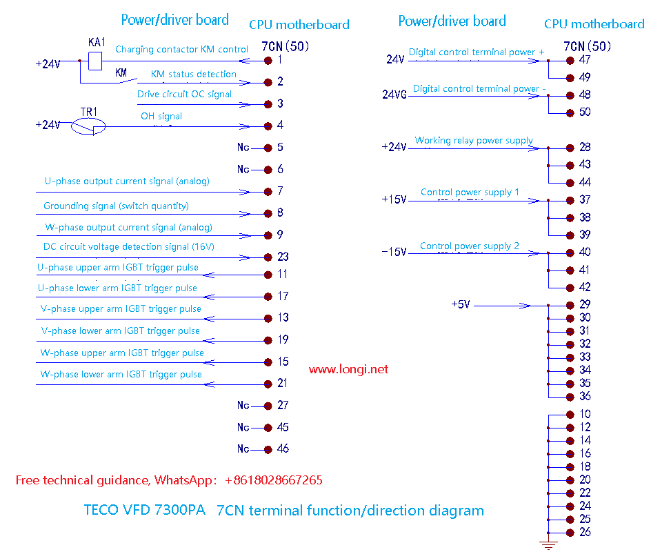
The above figure shows the function/destination (50 lines) of the TECO 7300PA inverter mainboard wiring terminal 7CN. The inverter of this model has excellent versatility in CPU mainboards, ranging from 22kW to 300kW, and can be interchanged. You only need to adjust the parameter “inverter capacity”. That is to say, this brand of inverter, due to different power levels, except for the power supply/driver board, actually uses the same CPU mainboard, so this terminal diagram can be used for “all sizes” during maintenance.
1. Check the input and output control signals. Most of them are switch signals, and the high and low level values are very obvious. For example, the detection signal terminals 2 and 4 of the charging contactor and temperature sensor have a terminal voltage of 24V when normal and 0V when abnormal. The static and dynamic (start/stop) voltage values of the six-way pulse signal terminals are obvious; although the output current detection signal is an analog quantity, it should be 0V when static and unloaded. Generally, it is about 2V when fully loaded.
2. You can “play tricks” on the terminals. For example, if the module overheats, you can try to short-circuit terminal 4 and pin 28. If the fault disappears, it means that the external temperature relay (sensor) at terminal 2 is faulty. If the fault still exists, it means that the fault is in the subsequent temperature signal processing circuit.
If you connect a potentiometer between terminals 10 and 29 and connect its center arm to the output current detection terminal (terminal 7 or 9), you can simulate a load test to check whether the subsequent current detection circuit is normal.
If an analog signal only deviates from the normal value (and still works), and falsely reports an “overvoltage” fault under normal power supply, you can use parallel and series resistance methods at terminals 23 to make its voltage value fall back to the normal detection value for emergency repair.
[ Failure Example 1 ] :
A 300kW7300PA inverter has an output frequency display on the operation display panel, but there is no three-phase voltage output on the U, V, and W terminals. After disconnecting the power supply of the inverter circuit, the six pulse signals of the 11, 13, 15, 17, 19, and 21 pins of the 7CN terminal were measured and all were normal. It was determined that the fault was in the pulse pre-stage signal circuit of the power supply/driver board. From these six terminals, it was quickly found that U12 (MC14069) was defective. After replacement, the fault was eliminated.
[ Failure Example 2 ] :
A 300kW7300PA inverter reported a “DC circuit undervoltage” fault after power-on and could not start running. The DC circuit voltage detection signal of terminal 23 of the wiring terminal 7CN was normal. After power-on, the measurement of terminal 2 was always low level, indicating that the auxiliary contact of the charging contactor was not closed. The CPU detected that the charging contactor was not closed, so it reported an undervoltage fault.
Try to short-circuit terminal 2 and terminal 28, and it runs normally.
Check from terminal 2 to the power supply/driver board and find out that the normally open contact of relay KA1 is connected in series in the 2-terminal circuit. The contact of KA1 is in poor contact. Replace KA1 and the fault is eliminated.
[ Failure Example 3 ] :
A 7300PA37kW inverter reported an OC fault as soon as it was powered on. The power supply of the current detection circuit was detected from the terminals. The -15V of terminals 40, 41, and 42 was 0V. Due to the abnormal power supply, the output of the current detection circuit was offset and an OC fault was reported. The -15V rectifier diode of the switching power supply was checked and found to be open. The fault was eliminated after replacement.
In the above three faults, with the guidance of the 7CN terminal diagram, the faults were found quickly and accurately in a very short time and the faults were eliminated efficiently.
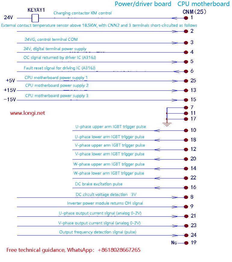
Figure 2.Alpha ALPHA2000 medium and small power inverter CNM motherboard wiring terminal function/direction diagram
The above picture is the Alpha inverter CPU motherboard CNM wiring terminal diagram, a total of 24 lines. Although the CPU motherboard of this model cannot be replaced – the overload protection and other parameters are fixed and the relevant parameter values cannot be modified; the CPU motherboard circuits are also different. I have seen two motherboard circuits, but the CNM terminals are the same. Therefore, the CNM terminal function/destination diagram is still very valuable as a “guide” for maintenance.
[ Failure Example 1 ] :
An Alpha 2000 15kW inverter tripped an undervoltage fault as soon as it was started, and no charging contactor closure sound was heard when it was powered on. The CNM terminal 1 was tested and was always at a high level of 24V, indicating that the charging relay control circuit was faulty. From terminal 1 to the CPU mainboard, it was determined that the circuit inside the CPU control pin was damaged.
Emergency repair: Short-circuit terminal 1 and terminal 7. After the switching power supply starts to oscillate, force the charging relay to be energized and closed to eliminate the fault.
[ Failure Example 2 ] :
An Alpha 2000 18.5kW inverter, with a load rate of less than 50%, but the on-site power supply fluctuates greatly, sometimes as low as 320V. The inverter tripped an undervoltage fault, and the dealer and the user required measures to make the inverter run. Cut the cable of CNM terminal 8, connect a 4.7kΩ semi-variable resistor between terminals 25 and 7 , connect the center arm to terminal 8, and adjust it to a fixed voltage of 3V.
The inverter no longer trips the undervoltage fault and operates normally. (This emergency measure must be used with caution in specific applications!)
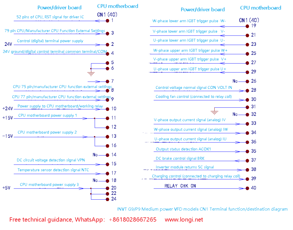
Figure 3.Function/direction diagram of CN1 terminal on INVT G9/P9 medium power inverter motherboard
There is a trick to speed up the inspection, which is to make a diagram of the motherboard wiring terminals. Clearly mark the terminal serial number and the source and destination of the terminal signal. It would be even better if the dynamic and static voltage values of each terminal could be marked. Fortunately, there are many switching signals, which are easier to detect and judge. Analog signals also have obvious differences in dynamic and static, which are easier to detect.
The figure above is the function/destination diagram of the CN1 terminal. For terminals 4, 7, 8, and 9, the terminals are set by the manufacturer. Except for replacing the CPU motherboard, you can check the short-circuited state of the terminals. For maintenance, it is useless, so don’t worry about it. 24V, +15, -15V, +15V, and +5V power supplies are the 5 power supplies commonly used by the CPU motherboard. Some inverters have two 24V power supplies, one for the control relay coil and the other for the control sub-power supply. The power supply introduction in the terminal occupies most of the terminals, six inverter pulses, and some have one DC braking pulse, which occupies part of the terminals. The others are various input/output, switch quantity/analog quantity signal terminals. What we need to pay attention to and frequently test is this third type of terminal. When checking a certain circuit, you can also artificially change the voltage state of this type of terminal to see if the corresponding circuit reacts. By observing or measuring the normal or abnormal reaction of the corresponding circuit, you can clearly judge whether the circuit is good or bad.
[ Failure Example 1 ] :
An INVT G9/P9 5.5kW inverter has an unbalanced output three-phase voltage. After disconnecting the inverter power supply, the start signal is input and the six pulse signal terminals 19, 21, 23, 25, 27 and 29 of CN1 are detected. It is found that the voltage at pin 21 is fixed and there is no change in dynamic or static state. It is judged that the fault is in the pulse pre-stage circuit or the PWM pulse output pin of the CPU.
Check the inverter pulse pre-stage circuit U4 (LS07), the six-way inverter pulse at the input end is normal, and there is no signal voltage output at the output pin 8. Replace U4 and the fault is eliminated.
[ Failure Example 2 ] :
An INVT G9/P9 5.5kW inverter reported an undervoltage fault during operation. The CN1 terminal 39 pin was detected to be low level, indicating that the CPU has output a charging relay closing signal. The charging relay was checked and found to have been replaced. The coil solder joints were poorly soldered. After re-welding, the fault was eliminated.
Fault Status: After powering on, the entire device does not respond, and the operation display panel shows no display. The measured 24V and 10V control power at the control terminals are both 0V.
Fault Essence: The VFD’s switching power supply is not working.
Troubleshooting Approach: (1) Switching voltage fault; (2) Pre-charging circuit fault.
Troubleshooting Method: (1) First check the power supply source of the switching power supply and whether the DC loop has a normal 530V voltage. If the DC loop voltage is 0V, it indicates a fault in the pre-charging circuit, such as an open charging resistor, damaged half-wave rectifier circuit, or poor contact of the normally closed contact of the contactor or relay. Repair the pre-charging circuit first and then check the fault of the switching power supply. Often, after repairing the pre-charging circuit, the VFD is also repaired. It is not necessary to focus too much on the switching power supply circuit at first.
(2) If the 530V, 265V, or 300V DC power supply for the switching power supply is available, do not focus too much on its voltage stabilization and oscillation circuit. First, check if there are any faults such as short circuits in the secondary load circuit of the switching transformer, such as a damaged cooling fan, an IC short circuit in the fault detection circuit, or a breakdown of the rectifier diode. The fault rate on the load side of the switching power supply is higher, while the problems in the oscillation and voltage stabilization links are less common.
The troubleshooting approach and order determine the efficiency of the repair work. From the perspective of the entire circuit, checking the pre-charging circuit is a very important step and should be the first consideration when troubleshooting the fault of a non-working switching power supply.
(B) Fault Inspection of the Inverter Pulse Circuit:
The section from the six PWM output terminals of the CPU to the intermediate buffer circuit is called the pre-stage circuit of the inverter pulse, while the drive circuit is referred to as the post-stage circuit of the inverter pulse, collectively known as the inverter pulse circuit.
Fault Conditions:
(1) Normal start-up operation, with normal output frequency indication on the operation display panel, but no three-phase output voltage. (2) Normal start-up operation, with normal output frequency indication on the operation display panel, but unbalanced three-phase output voltage. (3) OC fault occurs immediately after pressing the start button. (4) OC fault occurs during operation. (5) Light-load operation is normal, but motor with load jumps or encounters OC fault.
Essence of the Faults and Inspection Approach (Corresponding to the Five Fault Conditions):
(1) Several factors may contribute: a. Loss of +5V* power supply on the input side of the drive circuit’s optical coupler; b. Damage to the buffer of the pre-stage pulse circuit; c. Uncertainty of the CPU’s relevant control signals or damage to related control pins; d. Misoperation of the fault protection circuit, resulting in the locking of the pulse pre-stage circuit by the fault signal.
Special attention should be paid to the pre-stage circuit of the inverter pulse signal, such as tri-state triggers and buffer circuits, which may be directly controlled by voltage and current detection and protection circuits. When the protection circuit misoperates, it may clamp and block the transmission of six pulse signals. The concept of the fault protection circuit participating independently in pulse transmission control should be kept in mind. Although faults caused by a and b are more common, those caused by c and d often constitute difficult faults, and a lack of inspection approach in this regard may lead to detours in repair.
(2) Three factors may contribute: a. Damage to the opto-coupler of the drive circuit, preventing the normal transmission of inverter pulse signals; b. Increased internal resistance of the inverter module, leading to poor conduction in three upper-arm IGBT modules. Therefore, the three drive circuits may not be equipped with IGBT voltage drop detection circuits, resulting in a failure to report OC faults; c. Malfunction of the pre-stage pulse circuit or the CPU inverter pulse output pin, causing the inverter pulse to be missing in one or two channels.
Don’t focus solely on the post-stage drive circuit, as the inverter pulse of the pre-stage may not be input to the drive circuit. Especially, consider whether the module is faulty or the internal resistance of the inverter module has increased. Failing to consider factor c may also lead to difficult faults.
(3) Several factors may contribute: a. Defects in the post-stage drive circuit itself; b. Insufficient load capacity of the power supply of the drive circuit, such as loss of capacitance in filter capacitors and low efficiency of rectifying diodes (increased forward resistance and decreased reverse resistance); c. Defects in the inverter module.
Dynamic and static testing (voltage testing) of the drive circuit may appear normal, but it is necessary to test the current output capability of the drive circuit. Pay attention to factors b and c.
(4) Several factors may contribute: a. Load capacity of the drive circuit and internal resistance detection of the inverter module; b. Three-phase output current detection circuit; c. Reference voltage circuit in the fault detection circuit; d. User load-related reasons.
Pay attention to the influence of factors b, c, and d. Defects in the three-phase detection circuit itself or shifts in the operating point may cause false OC fault reports. Deviations in the reference voltage of the fault detection circuit may lead to inaccurate current detection and false OC fault reports. If all checks are fine, look for the cause on the production site, not excluding issues related to the load. Factors b and c may again fall into the category of difficult faults.
(5) Three factors may contribute: a. Insufficient current (power) output capability of the drive circuit; b. Defects in the inverter module, resulting in increased internal resistance; c. Issues with the load circuit, such as a faulty motor, not necessarily a fault of the VFD.
Abnormal operation of the VFD does not necessarily indicate a problem with the VFD itself. It is recommended that users try replacing the motor. Consider factors b and c, and sometimes factors outside the VFD.
In movies and TV shows, when a Taoist from Maoshan encounters an urgent and difficult situation, he often recites a curse: “The Supreme Old Lord is as sick as a law… If something difficult happens, it should be solved by the curse.”. If there is an urgent VFD repair, we can also recite a few mantras and find the “smart” method for quick maintenance. On a rainy day, thunder and lightning flash. The door of the maintenance department was suddenly forcefully pulled open by someone. Three or four strong men, carrying an unmarked 75kW VFD, strode in and asked, “Our workshop is for refining silver, and the frequency converter was damaged by lightning.”. Urgent use! Can the malfunction be detected and repaired within three hours. Okay, don’t bargain; If you don’t have diamond, don’t take on porcelain work. Let’s quickly change the door. It’s not just you who can fix VFD. This VFD may be able to earn half a month’s salary. No second words, fight!
I roughly inquired about the damage to VFD. During operation, due to lightning strikes introduced from the three-phase power supply, even the main power switch in the workshop tripped. Close the power switch of VFD again, there is a popping sound, and the switch jumps open again. In this situation, there must be a short circuit fault in the three-phase rectifier circuit of VFD. Instead of being busy with power on, use the resistance range of the multimeter’s R, S, T power input terminals and U, V, W output terminals to determine the resistance of the main circuit with the P and N terminals of the DC circuit. There is a short circuit phenomenon in the measurement, rectification, and inverter power circuits. Detailed inspection after disassembly revealed that two rectifier modules were damaged, one inverter module was broken, and the energy storage capacitor was tested and found to be fine. The repairman asked, “Isn’t it enough to replace these three faulty parts?”? Answer: Don’t be impatient. Due to the introduction of lightning strikes within VFD, the situation is complex and the quality of the control circuit board is unclear. If the inverter power module is damaged, it will have an impact on the driving circuit. If there is a hidden fault, the replacement module will be damaged again. Further investigation is needed to determine whether to replace the module. Key contents to be checked: 1. Whether the CPU motherboard is damaged, especially whether the CPU chip is damaged; 2. Inverter pulse transmission circuit, including driving circuit and inverter pulse front-end circuit. Especially for the driving circuit, the triggering terminal circuit of the IGBT should be checked for any open circuit or negative pressure power supply; 3. Other circuits, whether the control terminal circuit has been damaged by lightning strikes, and whether the control circuit (fault detection circuit, etc.) has been damaged. The key among them is that as long as the CPU can output six inverter pulses, repairing other faults should be easy.
(A) Power on the switch power supply or troubleshoot the switch power supply: Remove the CPU motherboard and power/driver board from the inverter casing and place them on the maintenance workbench. Power should be supplied to the switch power supply of the circuit board first, or the switch power supply should be repaired first to facilitate troubleshooting of other circuits. I tested the power supply terminals of the switching power supply and the filtering capacitor at both ends of the secondary rectification circuit of the switching transformer, and there was no short circuit phenomenon. It is possible to power on the switching power supply. The power supply source of the Shunxia switch power supply is directly taken from the 530V DC circuit of the DC circuit. If measured on the circuit, the drain (collector) of the switching transistor of the switching power supply should be connected to the P-terminal of the DC circuit, and the source (emitter) should be connected to the N-terminal of the DC circuit. Alright, connect the 500V DC maintenance power supply to the power supply terminal of the switch mode power supply (pay attention to polarity, it can be bad if connected in the opposite direction), it’s not bad! The corresponding changes in characters during the startup period on the operation display panel indicate that the switch power supply and the peripheral circuit of the CPU chip are basically working normally, and the CPU is also good. (B) Release the OH (module overheating) fault alarm: After the startup character on the operation display panel flashes, an OH (module overheat) fault code is reported. Press the RST reset button on the operation display panel, OH disappears once, and it is displayed again, unable to reset. At this time, the frequency converter is in a fault locked state and refuses to accept operating signals, making it impossible to detect whether the inverter pulse transmission circuit is normal. The OH alarm must be disarmed. Observing the main circuit, two normally closed contact type thermal relays are installed near the heat sink module. When the circuit board is disconnected from the main circuit, it is equivalent to the temperature sensor’s normally closed point breaking, reporting an overheat signal. Find the corresponding temperature sensor terminals on the circuit board, short circuit them with wires or solder, and there should be no OH fault reported. Some frequency converters use thermistors to detect the temperature of the module. When the terminal is open, an OH fault will also be reported. Simply remove the temperature sensor and insert it into the corresponding terminal on the control board. Still report OH, don’t worry, there may be related temperature detection signals sent to the control board. Observe the socket and lead of the cooling fan, which is a three wire fan. Two wires are the positive and negative terminals of the 24V power supply, and one wire is the signal wire. Return the operation/fault signal to the control board. If you remove the fan and plug it back into the control board, it would be too troublesome. There is a simple way to find the positive and negative wires, and test connecting the third wire to the positive and negative power supply terminals respectively. When this wire is connected to the positive power supply terminal, the OH fault code on the operation display panel disappears. (C) Release Uu (undervoltage) and input phase loss alarm: After a brief moment of joy, the operation display panel showed another Uu (undervoltage) fault, and the frequency converter was still in a fault locked state. When the switching power supply adopts 265V (or 300V) DC power supply, we disconnect the control board from the main circuit and separately supply 265V (or 300V) DC power to the switching power supply. Most of the operation panels will report Uu faults (some frequency converters, DC circuit voltage detection signals are obtained in the secondary rectification circuit of the switching transformer, so Uu faults will not be reported), because the input of the DC circuit detection circuit is in an open circuit state, and the circuit output is an undervoltage signal. From the DC circuit voltage introduction terminals (P, N terminals), find the input resistance network of the DC circuit detection circuit, a large high resistance circuit, seven or eight phases in series, because the switching power supply is 300V DC power supply at this time, directly introduce it into the DC circuit voltage detection circuit, or report a Uu fault. Short circuit a few resistors in the input resistor network (if there are 8 resistors, 3 can be short circuited for testing) to adapt to the 300V voltage output range. Introduce a DC voltage artificially into the DC detection circuit and modify the detection to meet the requirements of the voltage input range. Some frequency converters may not report Uu faults, but they may also report “charging contactor not engaged fault”, while others may still report Uu faults. Don’t worry, there may be related voltage detection signals sent to the control board. The charging contactor cannot be removed and connected to the control board in the main circuit. The frequency converter often has a status detection circuit for the auxiliary contact of the charging contactor. Due to the disconnection between the control board and the main circuit, the CPU detects that the auxiliary contact of the charging contactor is always in an open circuit state after the control board is powered on, and will also report Uu or “charging contactor not engaged fault”. Find the lead terminals of the auxiliary contacts of the charging contactor from the main circuit, determine the corresponding socket terminals of the control board, short circuit or solder the lead terminals with wires, and tell the CPU that the charging contactor has been closed. After short circuiting the lead terminals of the auxiliary contacts of the charging contactor, the operation display panel finally stopped tripping Uu fault. (D) Release OC (module overcurrent or output short circuit) fault alarm: After a brief moment of joy, the fault code no longer jumps. From the display on the operation display panel, it appears that the inverter has entered standby mode and can be started for maintenance of the inverter pulse transmission channel. Press the start/stop button on the operation display board, but the frequency converter does not respond. The user may have set it to terminal operation. Ask the repairman, and indeed. For the convenience of operation, if the control parameters can be modified (if there is a frequency converter manual at hand), or the operation can be changed to start/stop and frequency adjustment using the control panel; If it is inconvenient to modify the parameters, you can try inputting the operation and frequency signals from the control terminal. Measure the frequency and adjust the power supply to 10V for normal output. Short circuit it to the input end of the 0-10V frequency signal to input the highest operating frequency command for the frequency converter (it is not troublesome, but can also be adjusted with an external potentiometer). Short circuit the forward running terminal to the digital common terminal for a startup test, and the operation display panel will display an OC fault code. Of course, the frequency converter is still in a fault locked state and cannot accept the operation. The power module cannot function without various comprehensive protections, but at this point, I really feel that these fault alarms are troublesome. However, if they are not resolved, the inverter pulse transmission circuit cannot be repaired. Slowly, when an alarm signal is issued, it will be tracked and released. Generally, when the control circuit board is disconnected from the main circuit, three or four faults will jump out. Pay attention to finding the source of each signal from each plug-in terminal, or from the input and output sides of the plug-in terminal or the optocoupler that transmits the signal, use wire short circuiting method to force the CPU to input a “normal” signal and release the fault lock state. The OC signal is mostly sent back to the CPU by the IGBT voltage drop detection circuit (IGBT protection circuit) of the driving circuit. When there is a fault in the output current detection circuit, an OC fault will also be reported, but this situation is relatively rare. Following the principle of easy first and difficult later, the OC signal returned by the driving circuit can be released first, and then the output current detection circuit can be detected. The commonly used ICs for driving circuits are PC923, PC929, and A316J. The former uses the OC signal output by the internal IGBT protection circuit of PC929, which is then sent to the CPU through an external optocoupler. Find the optocoupler connected in parallel with PC929, and short-circuit its input side with a soldering iron to release the OC alarm (it is a fast method, not a good method); The latter, the 5 pins of the driver chip A316J are the OC signal output pins, which are separated from the copper foil strip to isolate the transmission of OC signals; But this method is not very convenient. Although it blocks the transmission of OC signals, it is advisable to check whether the CPU and the front-end inverter pulse transmission circuit have output inverter pulse signals. However, the drive IC itself is still in a fault locked state, which is not conducive to repairing the drive circuit. A good solution is to manually input an IGBT “normally open” signal to the IBGT detection circuit, so that the driving IC itself no longer reports OC faults during the input inverter pulse period. The general driving circuit is implemented by the lower three arm driving circuit to detect the voltage drop of the IGBT transistor. The trigger terminal is used to short circuit the output end of the inverter pulse to the OV end of the driving power supply (the connection point with the N end of the main circuit), which is also relatively easy to find. (E) Perform maintenance on the drive circuit: Finally, the frequency converter can accept the startup signal. Looking at the gradually increasing output frequency indicator displayed on the control panel, I breathed a sigh of relief, indicating that the CPU circuit and control terminal circuit are both good. The repair of the frequency converter is basically without any suspense. Measure the six inverter pulse input terminals of the driving IC, and there is a significant voltage change in the start and stop states. The six inverter pulses from the CPU motherboard have been input into the driving circuit intact and undamaged. The CPU motherboard is good! Measure the output status of six inverter pulses from the pulse output terminals of the power/driver board, and check if the negative cutoff voltage is normal and if there are normal pulse outputs. Does the voltage amplitude and current amplitude of the pulse output meet the normal requirements? Due to the damage of the IGBT causing impact on the driving IC, there are two driving circuits that cannot output pulse signals normally. This is simple. A power amplifier consisting of a driver IC and a rear stage consisting of two transistors was found to have damaged components. After replacement, all six inverter pulses were output normally. The maintenance process has been declared completed. The entire maintenance process took exactly 45 minutes. After the maintenance is completed, it seems like we won a small battle so happily. The next task is to replace and purchase modules.
Throughout the entire maintenance process, four strong men were eagerly staring at the frequency converter, including one electrician who was extremely excited: he had learned and really had real skills. I didn’t expect it to be so troublesome. Blowing up a module is not as simple as replacing it. To the repairman, the control circuit has been repaired, but there is no power module at hand. Then, you can go to the same city to “search” for it. If not, it will only be sent from outside the city. You will have to find your own way to delay your silver refining. The four repairmen all laughed and said, “No problem, no problem. Please hurry up and send the package.”. The various methods used during the maintenance process are scattered in my other blog posts, but they belong to local maintenance methods. For actual maintenance, sometimes there is a small gap between what is explained by a single unit circuit, which is difficult to understand. Through the description of a specific maintenance example process in this article, the application of various maintenance methods can be integrated and integrated.
The main circuit of the fault detection circuit is still composed of an operational amplifier. Usually, the operational amplifier is connected to the following types of circuits, completing three tasks of signal analog amplification, comparative output, and precision rectification. (A)、 Inverting amplifier circuit:
An operational amplifier has excellent characteristics such as high input impedance (without using signal source current), low impedance (with good load characteristics), amplification of differential mode signals (the difference between two input signals), suppression of common mode signals (with the same polarity and size of the two input terminals), and the ability to provide linear amplification for both AC and DC signals. The figures (1), (2), and (3) in the circuit form are inverting amplifiers, where the output signal is in opposite phase to the input signal, also known as inverting amplifiers. The circuit has a dual amplification effect of voltage and current on the input voltage signal, but in small signal circuits, only the amplification and processing of the voltage signal are emphasized. The voltage amplification factor of a circuit depends on the ratio of R2 (feedback resistance) to R1 (input resistance). R3 is the bias resistor, and its value is the parallel value of R1 and R2. Due to the different values (ratios) of R2 and R1, three types of signal transmission functions can be completed, namely, forming three signal processing circuits: inverter amplifier, inverter, and attenuator. (1) The circuit is an inverting amplifier circuit with an amplification factor of 5; (2) The circuit is a inverter, which plays a reverse phase output role on the input signal and has no amplification factor, so it cannot be called an amplifier. Or input a 0-5V signal, then output a 0-5V inverted phase signal; (3) The circuit is an attenuator circuit. If a 0-10V signal is input, the output is 0-3. A 3V inverted signal is a proportional attenuator. Figures (1), (2), and (3) have two characteristics of the circuit: 1. The input and output signals are reversed; 2. Whether it is an amplification, attenuation, or inverting circuit, the output signal maintains a proportional output relationship with the input signal, which can be broadly referred to as an inverting amplifier because the amplification factor of the inverter is 1, and the attenuator precisely utilizes the amplification effect of the circuit. It is interesting that these three types of inverting amplifiers have applications in current and voltage detection circuits. Taking the current detection circuit as an example: This is because the current transformer connected in series to the three-phase output terminal has an amplifier built-in, and the output signal has reached a voltage amplitude of volts, while the input signal amplitude of the CPU must be within a voltage amplitude of 5V or less. Therefore, some reverse current signal processing circuits use reverse amplifiers with a certain amplification factor; Some use inverter circuits, which only perform inverter processing on the signal based on the polarity requirements of the CPU input voltage signal, without the need for further amplification; Some circuits are adapted to the signal amplitude range of the later stage circuit, and even use attenuator circuits to attenuate the voltage signal from the current transformer before sending it to the later stage circuit. The power supply of the analog signal circuit in the detection circuit is generally powered by both positive and negative 15V dual power sources according to the requirements of amplifying AC signals. Based on the circuit form of the inverter amplifier and the circuit characteristics of the operational amplifier, we can find the corresponding detection method:
According to the characteristics of the inverting amplifier, when a positive signal voltage is input, the input voltage must be negative below 0V, and vice versa, the output voltage must be positive above 0V, with 0V (ground) as the reference potential. To determine whether it is in a normal state based on the static circuit values of the circuit and input/output pins;
Identify whether the circuit in this stage is an amplifier, inverter, or attenuator. Based on the ratio of input resistance to feedback resistance, the output voltage value can be roughly calculated to determine whether the circuit is in a normal state;
According to the characteristic that the circuit has an amplification (or attenuation) effect on differential mode signals and a zero amplification effect on common mode signals, when short circuiting two input terminals, the output voltage should be close to the zero potential value; Alternatively, if there is a positive voltage (or negative voltage output) at the output terminal, but two input terminals are short circuited, the output voltage immediately drops (or rises) to around 0V. The circuit is good and can transmit signals normally.
If the input voltage value can be artificially changed, the output voltage will inevitably change accordingly, which can be used to determine whether the amplifier is in a normal state. [Fault Example 1] After a certain frequency converter is powered on, an OC fault is reported, and the fault reset is invalid. The current detection circuit, as shown in the diagram (1), has an output voltage of+12V. The CPU reports an OC signal after power on due to a serious overcurrent signal input. Short circuit the 2 and 3 pins of the operational amplifier with metal tweezers, measure that there is no change in the output circuit of pin 1, and it is still+12V. It is judged that the operational amplifier is damaged. After replacement, the fault is eliminated. [Fault Example 2] A certain frequency converter outputs an undervoltage signal after being powered on, and detects the electrogram (2) circuit. The input voltage is -3V, but the output voltage is 0. 7V, indicating a malfunction of the amplifier in this stage. A 10k resistor was connected in series with an external DC 12V power supply, and the output voltage did not change when input to the reverse input terminal. It was determined that the amplifier in this stage was damaged, and the fault was resolved after replacement. (B)、 In phase amplifier and voltage follower circuit:
In phase amplification circuit and voltage follower circuit
The circuit shown in Figure (1) is a typical circuit form of a in-phase amplifier, which is also one type of amplifier circuit. The input signal enters the same phase end of the amplifier, and the output signal is in the same phase as the input signal. The voltage amplification factor of the circuit is 1+R2/R1. It is also used for amplifying analog signals in fault signal detection circuits. When R2 is short circuited or R3 is open circuited, the output signal has the same phase and equal magnitude as the input signal, so (1) the circuit can further evolve into (2) and (3) circuits. The above figures (2) and (3) show the voltage follower circuit. The output voltage completely tracks the amplitude and phase of the input circuit, so the voltage amplification factor is 1. Although there is no voltage amplification effect, it has a certain current output ability. The circuit plays a role in impedance transformation, improving the load capacity of the circuit and reducing the mutual influence of high impedance in the signal input circuit and low impedance in the output circuit. When used as a circuit follower, sometimes a single power supply is also used. (1) The circuits (2) and (3) are also used in fault detection circuits for amplifying analog signals and processing reference voltage signals. Based on the characteristics and functions of the circuit, the detection method can be obtained as follows:
(1) The circuit is a in-phase amplifier circuit, and the output voltage amplitude and polarity are proportional to the input voltage. The voltage amplification factor of this stage is about 6 times. When the input voltage value is 1V, the output voltage is approximately 6V. It is possible to determine whether the circuit is in a normal state based on the calculation of input and output voltage values;
(2) (3) The circuits are all voltage follower circuits, and the output voltage is completely tracked by the input voltage. The output voltage should be equal to the input voltage, which can be used to determine whether the circuit is in a normal state.
By short circuiting two input terminals or manually changing the input voltage, the corresponding changes in the output voltage can be measured to determine whether the circuit is in a normal state. [Fault Example 1] A certain frequency converter experienced an OH fault when powered on. The reference voltage circuit of the temperature detection circuit, as shown in Figure (2), has an output voltage of 1V. This machine is a voltage comparator circuit, and its input voltage is measured to be 5V. Under normal conditions, the output voltage should also be 5V. After cutting off the output load circuit, the output voltage remains at 1. 2V, it was determined that the amplifier in this stage was damaged, and the fault was resolved after replacement. (C) Precision positive and negative half wave rectifier and full wave rectifier circuits:
Precision half wave and full wave rectifier circuits
The AC voltage signal from the current transformer needs to be rectified into DC voltage through subsequent half wave or full wave rectification circuits, and then sent to the CPU for current display and control. Precision half wave or full wave rectification circuits are also used for processing and amplifying analog signals. Ordinary rectification circuits use diodes as rectification devices, but diode rectification has drawbacks such as nonlinear distortion and dead zone voltage. Especially when used for small signal rectification, it will cause output signal distortion and output errors. By utilizing the amplification effect and deep negative feedback effect of the operational amplifier, a diode is added to the amplification circuit. By utilizing the unidirectional conductivity characteristics of the diode, different depths of negative feedback are introduced to the input positive and negative half wave signals. The input μ V level signal can be rectified in a dense manner, and the circuit itself also has a voltage following or amplification effect. The above figure (2) shows a precision negative half wave rectification circuit. The circuit will perform precision rectification on the input negative half wave signal and output it in reverse phase. For the positive half wave input signal, the connection of D1 introduces deep negative feedback to the amplifier; At the beginning of the negative half wave input signal, due to the signal input amplitude being smaller than D1 and D2, both are in the cut-off state, and the circuit is in an open-loop amplification state. A small signal input will cause the output pin voltage to be greater than -0. 7V, D1 conduction, D2 reverse bias cutoff; The series connection of D2 and R125 introduces moderate negative feedback (the resistance of R125 can determine whether the current circuit is a rectifier or a rectifier amplifier, and the current circuit is a precision rectifier with no amplification effect), which is equivalent to an inverter amplifier, and the output is inversely correlated with the input signal. The difference between the circuit in Figure (1) and Figure (2) is that the polarity of the two diodes in the circuit is opposite, making it a precise rectification circuit for the input positive half wave signal. The principle of rectification is the same. By adding a half wave rectifier circuit and an inverse summation circuit, as shown in Figure (3), the positive and negative half waves are input and output in reverse to obtain a full wave output voltage waveform, forming a high-precision full wave rectifier circuit. In fault detection circuits, rectifier circuits are often used to sample the three-phase output current signal, which is rectified and amplified as an analog voltage signal (current detection signal) input into the subsequent fault signal processing circuit and CPU circuit, used for overload alarm and sampling processing of operating current. The input of the circuit is an AC voltage signal, while the output is a DC voltage signal. Most circuits are rectifiers, and some circuits are rectifier amplifiers. Detection method:
Rectifier circuit: The input side is AC voltage, and the output side is DC voltage. The two measured values are relatively close.
Rectifier amplifier, with AC voltage on the input side and DC voltage on the output side. The output DC voltage value is higher than the input AC voltage value.
By short circuiting two input terminals or manually changing the input voltage, the corresponding changes in the output voltage can be measured to determine whether the circuit is in a normal state. [Fault Example 1] A certain frequency converter experienced an OC fault when powered on. The output voltage of the current detection circuit as shown in Figure (2) was 13V. After unplugging the lead terminal of the current transformer, the amplifier in that stage still had 13V. It was determined that the rectifier circuit was damaged and the fault was resolved after replacement. (C) Circuit for voltage comparator, step voltage comparator, and window voltage comparator: The above-mentioned circuits are all used for amplifying and rectifying analog signals, and their output signals still have analog signals, which can be called analog signal (amplification) processing circuits. However, in the following voltage comparison and other circuits, the output is a switch signal. The circuit has left the scope of analog amplification and seems to have entered the field of “digital circuits”, using analog circuits as digital circuits for application.
Three types of voltage comparator circuits
The function of a voltage comparator is to compare the magnitude of two input voltage signals. In Figure (1) of the circuit, the voltage at the same phase input end of the amplifier is the voltage divider value 2 of R2 and R3 resistors to+5V. 5V, known as the reference voltage value, compares the input signal with this reference value. When it is higher than this value, it outputs a 0V low-level signal. When it is lower than the low value, it outputs a+15V high-level signal. Circuit, also known as a single value comparator, the output state of the circuit depends on a value (a point) of the input signal voltage -2. 5V. If the two-stage voltage comparator is connected to the circuit shown in Figure (2), it becomes a stepped voltage comparator. The circuit has one input signal and two output signals. The N1 and N2 voltage comparators input the same signal voltage, but the reference voltage values at the same phase input terminals of the two-stage circuit are different. The N1 reference voltage is 6. The reference voltage value for 6V and N2 is 3. 3V. When the input signal gradually increases from 0V to 3. When the voltage is above 3V, the output state of N2 first changes to low level; N2 has an input signal value greater than 6. At 6V, there is only a low-level signal output. When the circuit in Figure (2) is used for voltage detection in the DC circuit, when the regenerative energy generated by the load motor is fed back to the DC circuit, causing the DC circuit voltage to rise to a certain value, N2 first outputs a braking action signal, connects the braking resistor to the DC circuit, and consumes the voltage increment; If the voltage continues to rise, N1 will output an OU overvoltage signal, and the frequency converter will shut down for protection. If the two-stage voltage comparator is connected to the circuit shown in Figure (3), it constitutes a window voltage comparator circuit. Compared to single-stage voltage comparator circuits, window voltage comparators can be referred to as dual value comparators. The circuit has two benchmark comparison values and outputs one signal. When the input signal is ≥ reference voltage 1 ≤ reference voltage 2, the circuit output state transitions. Within a range of the intermediate value of the input signal, the output state remains unchanged. The circuit in Figure (3) is a ground fault signal processing circuit. The in-phase end of the N1 amplifier is the voltage divider of R46 and R50 to+15V, while the reverse end of the N2 amplifier is the voltage divider of R81 and R69 to -15V. The input three-phase current sampling signal enters the reverse input terminal of N1 and the in-phase input terminal of N2, and is compared with the positive and negative partial voltage values, respectively. Whether it is the positive half wave or negative half wave of the input signal, as long as it is greater than the two reference values, a ground short circuit signal will be reported. The voltage comparator uses digital circuits, which can flexibly set the reference voltage based on the signal amplitude, making it more convenient than using digital circuits. In addition, the circuit in Figure (3) adopts an operational amplifier circuit with an open collector output, which can achieve parallel output at the output end, making the circuit more concise. If a regular amplifier is used, the output signal also needs to be isolated by two diodes and connected together in parallel. Three types of voltage comparator circuits are commonly used to convert analog signals of detected current or voltage into switch signal – fault signal output, for implementing control actions and shutdown protection. Detection method:
The amplifier output has only two level states, low level, close to the ground level of the power supply or negative power supply value; High level, close to positive power supply value;
If the voltage value of the inverting input terminal is lower than that of the in-phase input terminal, the output is low level; otherwise, the output is high level.
By short circuiting two input terminals or manually changing the input voltage, the corresponding changes in the high and low levels of the output terminals can be measured to determine whether the circuit is in a normal state. (E) Hysteresis comparator circuit: It is also one of the voltage comparator circuits. The circuit in Figure (3) of the voltage comparator, also known as the hysteresis voltage comparator circuit. The voltage comparator circuit can be upgraded to a hysteresis comparator circuit by introducing an additional positive feedback circuit. Hysteresis comparator circuits are referred to as voltage comparator circuits with hysteresis characteristics. If ordinary voltage comparison is regarded as “voltage point comparison”, hysteresis comparator can be regarded as a comparator circuit for “voltage range comparison”. Usually, we hope that the output state of the circuit is stable enough, and comparing the voltage at a “point” can cause instability in the output state due to frequent output. Improving the “point” comparison of the input circuit to “segment” comparison can effectively solve this problem – within a “segment value” of input voltage variation, the output state remains unchanged. Figure (2) shows a positive feedback branch composed of R4 and D1, which converts the “point” comparison characteristic of the circuit into a “segment” comparison characteristic.
The control principle is briefly described as follows: Assuming that the circuit in Figure (2) is used for processing the braking action signal, the input signal is the voltage sampling signal of the DC circuit. When the voltage of the DC circuit rises abnormally due to the energy feedback from the load motor, reaching 680V, the input voltage value of Vin reaches 9. When the voltage is above 5V and higher than the reference voltage at the reverse end of the amplifier, the amplifier outputs a low-level signal, and the subsequent braking circuit acts, connecting the braking resistor to the DC circuit to consume the voltage increment; Due to the consumption effect of the braking resistor, the input voltage value of Vin quickly drops to 9. Below 5V, but the braking signal is still being output, and it does not mean that the DC circuit voltage slightly drops, causing the braking signal to disappear. This indicates the role of the hysteresis comparator. The braking circuit continues to operate until the DC circuit voltage returns to below 620V, and the sampled input voltage is below 7. The braking circuit only stops working at 5V. When the circuit is static, the voltage at the same phase end of the amplifier (7.5V) is higher than the voltage at the opposite phase end, and the output voltage is a high-level voltage of nearly 15V. R4 and D1 are introduced into the same phase end circuit, artificially raising the same phase end voltage to 9. 5V. When the input voltage is above 9. At 5V, the circuit output state reverses and the output end becomes low level. D1 reverse bias cutoff, feedback loop interruption, and reference voltage at the same phase end restored to 7. 5 V partial voltage value. In this way, when the input sampling voltage is below 7. At 5 V, the brake signal stops outputting. Hysteresis comparator circuits are commonly used for voltage detection in DC circuits, outputting braking signals and overvoltage/undervoltage fault signals. The detection method is the same as the voltage comparator, omitted.
The voltage amplitude of the six driving pulses outputted by the driving circuit meets the requirements. For example, measuring the amplitude of the positive excitation pulse voltage in the AC range is about 14V, and the amplitude of the negative cutoff voltage is about 7.5V (different models may vary). After the above inspection of the driving circuit, most maintenance personnel believe that the machine can be installed, but an extremely important inspection step – the inspection of the current (power) output ability of the driving circuit! Many VFDs that we believe have been repaired normally will still expose more hidden faults during operation, leading to a certain repair rate.
VFD operates normally under no-load or light load, but after carrying a certain load, it may experience motor vibration, output voltage phase deviation, frequency jump OC faults, etc. Cause of malfunction: A. Insufficient output capacity of the power supply current (power) of the driving circuit; B、 The driving IC or the post amplifier of the driving IC is inefficient, and the output internal resistance increases, resulting in insufficient voltage or current amplitude of the driving pulse; C. IGBT is inefficient, with increased internal resistance and increased pressure drop in the conduction tube.
The proportion of failures caused by reason C is not high, and is limited by the conditions of the maintenance department, such as the inability to provide rated load testing for the frequency converter. But for the hidden faults caused by reasons A and B, we can use the method of increasing the load on the driver to expose them and then repair them, which can reduce the repair rate to the lowest level. The normal opening of IGBT requires not only sufficient excitation circuit amplitude, such as+12V or above, but also sufficient driving current to ensure its reliable opening, or to ensure its conduction under a certain low internal resistance. The essence of the causes of faults A and B mentioned above is that due to the insufficient power output capability of the driving circuit, although the IGBT can be turned on, it cannot be in a good low conductivity internal resistance state, resulting in output phase deviation, severe motor vibration, and frequency jump OC faults.
Let’s conduct a more in-depth analysis of the control characteristics of IGBT and identify the root cause of the fault.
I. Control characteristics of IGBT: The common perception is that IGBT devices are voltage-controlled devices, which require a certain level of excitation voltage for gate bias control, without the need to draw excitation current. In low-power circuits, only digital gate circuits can drive MOS-type insulated gate field effect transistors. As an IGBT, the input circuit happens to have the characteristics of a MOS-type insulated gate field effect transistor, and can therefore also be considered a voltage-controlled device. This perception is actually biased. Due to structural and process reasons, a junction capacitance called Cge is formed between the gate and emitter junctions of the IGBT tube, which controls the turn-on and turn-off of the IGBT tube. In fact, the charging and discharging control of Cge is responsible for the control of the turn-on and turn-off of the IGBT tube. The +15V excitation pulse voltage provides a charging current path for Cge, which turns on the IGBT; the -7.5V negative pulse voltage “forcibly pulls out the charged charge” on Cge, which plays a role in rapidly neutralizing the charged charge, and turns off the IGBT. Assuming that the IGBT tube only controls the on-off switching of a DC circuit with a zero operating frequency, and after the Cge is fully charged at one time, there is almost no need for charging and discharging control, it is reasonable to describe the IGBT tube in this circuit as a voltage control device. However, the problem is that the IGBT tube in the output circuit of the frequency converter operates at a frequency of several kHz, and its gate bias voltage is also a pulse voltage with a frequency of several kHz! On the one hand, for such high-frequency signals, the capacitive impedance exhibited by Cge is relatively small, resulting in a large charging and discharging current. On the other hand, to make the IGBT turn on reliably and quickly (striving to make the tube have a small internal resistance), it is necessary to provide as large a driving current (charging current) as possible within the allowable operating range of the IGBT. For the control of turn-off, it is also the same. It is necessary to provide a low-resistance (ohmic) external discharge circuit to discharge the charge on the gate-emitter junction capacitor very quickly! As we all know, capacitors are energy storage components that do not consume power themselves, and are called capacitive loads. However, just like the principle of power transmission and distribution lines, in addition to the power supply having to provide reactive current (reactive power) for capacitive components, which increases the power capacity of the power supply, the reactive current inevitably brings losses in line resistance (line loss)! The power loss of the drive circuit mainly concentrates on the gate resistance and the conduction internal resistance of the final amplifier tube. We often see that the output stage of the drive circuit, especially for high-power VFDs, is actually a power amplifier circuit, often consisting of medium-power or even high-power transistors, several watts of gate resistance, and other components, indicating that the drive circuit of IGBT consumes a certain amount of power and needs to output a certain current. From the above analysis, it can be seen that the IGBT tube used in the VFD output circuit should be a current or power drive device, rather than a pure voltage control device
II. The last testing content before installation: To minimize the rate of rework, after conducting comprehensive testing on the drive circuit in sections 3 and 4, do not miss the inspection of the drive circuit’s load-bearing capacity. The method is as follows:
Measurement circuit for driving circuit with load capacity
The above diagram shows the driving circuit of the U-phase upper arm of DVP-1 22kW Delta VFD. The GU and EU in the figure are pulse signal output terminals, which are externally connected to the G and E poles of the IGBT. When repairing the drive board, it has been disconnected from the main circuit. The dashed box represents the external measurement circuit. After powering on the power supply/driver board, in conjunction with start and stop operations, a DC 250mA current range is connected in series at points m and n, and an external measuring resistor of 15 Ω 3W forms a circuit to detect the current output capability of each drive circuit. The starting state is measured, and five output current values are all around 150mA, with one output current only 40mA. The reason for the OC trip after installation and operation is precisely because the driving capability of this drive circuit is greatly insufficient! In the shutdown state, the measured current output capacity of each negative voltage power supply is about 50mA, and the negative voltage power supply capacity is normal. Connecting RC in series plays a current limiting role, and the principle of its value is to select resistance and power values that are equal to the gate resistance (the parameter value of DR45 in the above figure) to make the detection effect obvious. After testing the power output capability of the driving circuit, it can be determined that the driving circuit is completely normal. During the testing process of connecting the drive circuit to the main circuit, please first use a low-voltage 24V DC power supply to power the inverter circuit. After testing the drive circuit and inverter circuit to be normal, restore the normal power supply to the inverter circuit. If there is no low-voltage DC power supply at hand, at least two 45W light bulbs or 2A fuse tubes should be connected in series in the inverter power supply circuit. After the machine is tested normally, the original power supply of the inverter circuit should be connected! The above power on detection of the driving circuit is carried out after disconnecting from the main circuit (IGBT). When the whole machine is connected, the input and input sides of the driving circuit must not be measured. Interference signals may be introduced due to human body induction and meter probes, causing IGBT to be triggered and conduct incorrectly, resulting in module explosion!
The insufficient output capability of the driving circuit is caused by two reasons: A、 The power supply capacity is insufficient. Under no-load conditions, when we detect the output positive and negative voltages, they often reach the normal amplitude requirements. Even under load (such as after connecting to IGBT), although the instantaneous charging capacity of Cge is insufficient, due to the short charging time, we often cannot measure the low voltage drop of the power supply. Without resistive loads, this hidden fault can hardly be detected! The common fault in the circuit is the loss of capacitance of the filtering capacitor, as shown in DC41 in the figure above. Due to the drying up of the electrolyte inside the electrolytic capacitor during long-term operation, its capacity has decreased from a few hundred microfarads to several tens of microfarads, and even to a few microfarads. In addition, there may be inefficient rectifier tubes, such as an increase in forward resistance, which can also cause insufficient power output capacity; B、 The internal output circuit of the driving IC is poor, or the internal resistance of the rear amplifiers DQ4 and DQ10 increases due to conduction. If there is no low drop in the power supply voltage after load testing, and the output voltage of T250 is detected to be low, it is a T250 defect. Otherwise, replace components such as DQ4 and DQ10. The phenomenon of increased resistance values such as DR40 and DR45 is relatively rare. It should be noted that the insufficient positive excitation voltage only manifests as severe motor vibration, output voltage phase deviation, frequent OC faults, and other phenomena. Although it may cause overcurrent in the DC component of the motor winding, it poses a danger to the module structure that cannot be put into operation and the signal will burst. The loss of the negative cutoff voltage (caused by a fault in the negative pressure power supply circuit, which blocks the negative gate bias circuit) indicates that it is normal when powered on. When the start button is pressed, the IGBT inverter module will emit a “pop” sound and immediately burst into failure! Why is this?
III. Hazards of IGBT cut-off negative pressure circuit open circuit: Except for the damage caused by sudden short circuit of the load during full speed operation, the harm of all faults such as overcurrent, overload, and undervoltage is far less than the harm of open circuit of gate bias circuit to IGBT. Speaking of this, maintenance personnel will deeply understand that they should not suffer too much from such losses. During the maintenance process, the gate resistor DR45 was missed, and during the installation process, only the trigger plug of the upper arm IBGT1 was carelessly inserted, forgetting to connect the lower arm IGBT trigger terminal, resulting in the IGBT2 drive signal introduction terminal being vacant. After power on, the start signal is not activated, and there is no problem. Once the start signal is activated, there is no discussion, and the module is damaged. In my long-term maintenance work, I have developed a habit of stopping for a while before starting the operation after powering on, and observing whether the drive pulse output terminal is properly connected. After checking that each connection is intact, press the start button again. I often feel that this slight point is of great importance – the driving circuit and inverter output circuit are both in a normal state, and only one signal terminal of the driving pulse is missing, which will inevitably cause serious damage to the IGBT module and driving circuit again, resulting in all previous efforts being wasted!
Equivalent diagram of IGBT junction capacitance
Just like bipolar devices – transistors, three wire components inevitably form three equivalent capacitors inside, while the Cge inside IGBTs is not parasitic, but formed by process and structure. Let’s not bother with Cce capacitors. The two capacitors, Ccg and Cge, can have a destructive effect on IGBT. The above diagram shows the situation when the triggering terminal of the lower arm IGBT is open circuit. After power on, IGBT1 can maintain a reliable cut-off state by applying a negative cut-off voltage to the G and E poles due to the connection of the driving circuit. The reckless input of the frequency converter operation signal causes IGBT1 to be driven by a forward excitation pulse voltage and turn on. The C pole of IGBT2, the U terminal, immediately jumps to a DC high voltage of+530V. This jump voltage provides a charging return circuit for the Ccg and Cge capacitors. During the turning on period of IGBT1, IGBT2 is also driven by this charging current, and it is almost simultaneously turned on. The common connection of the two tubes forms a short circuit to the+530V power supply at the P and N terminals. With a loud bang, both tubes explode! If the signal terminal of the upper tube is empty and the lower tube is connected to the driving circuit, the conduction of the lower tube will also cause damage to both tubes for the same reason. Assuming that there is a gate bypass resistor connected in parallel on the G and E poles of IGBT2 (such as the R side in the IGBT1 gate control circuit), it will form a bypass effect on the charging current mentioned above, and the possibility of the two transistors sharing the same circuit will be reduced. Assuming that during the conduction period of the upper tube, there is a cut-off negative pressure of about 7V between the G and E terminals of the lower tube, and the positive charging current is neutralized and absorbed by the gate negative bias, which is far from reaching the amplitude required to turn on the IGBT, then IGBT2 is safe. This is also why negative pressure is added to the control circuit of IGBT. For frequency converters using IPM intelligent inverter modules, the driving power supply is often a single power supply without providing negative pressure. Is that the case? From a design perspective, the shorter the lead of the IGBT drive signal, the better, in order to reduce the inductance effect of the lead; There should be a small resistance circuit between the E and E poles of the IGBT to fully bypass the interference signal current. The IPM module, driver circuit, and inverter main circuit are integrated inside the module, and the wiring between the driver circuit and IGBT is extremely short. According to data, even the gate resistance is omitted to reduce the wiring impedance. In the off state, IGBT ensures that the gate is in a low impedance grounded state, effectively preventing misleading conduction caused by interference signals, thus eliminating the need for negative power supply.