Posted on Leave a comment

Siemens MM430 VSD 7.5kW power supply hiccup fault

Repair an imported Siemens 7.5kW frequency converter due to power supply hiccup fault, with no display on the operation panel. Due to its special installation structure, the machine is surrounded by three circuit boards and a heat dissipation plate in a square shape, with an embedded shell. When repairing, it is necessary to disconnect the circuit board and lay the entire circuit flat on the workbench, such as unfolding a roll of ancient bamboo slips, in order to facilitate maintenance. Moreover, the circuit board is a four layer board, making circuit maintenance difficult.

Starting from the switch power supply circuit, first use the elimination method to cut off the load circuit one by one. If it still cannot vibrate well, it indicates that hiccups are not caused by excessive load. There are no abnormalities in the oscillation and voltage stabilization circuits. Finally, it was found that two 200V voltage stabilizing tubes in the cut-off shunt circuit of the switch tube were damaged due to breakdown. We purchased 110V voltage stabilizing tubes from the market and replaced them with four to repair them. A typical shunt (also known as anti peak voltage absorption) circuit uses a diode connected in series with a resistance capacitance parallel circuit, and then connected in parallel with the primary winding of a switching transformer. The diode connection method is similar to the freewheeling diode connection method of a typical coil circuit. Its function is to quickly release the electrical energy of the primary winding circuit during the period when the switching transistor is approaching cutoff, so that the switching transistor can cut off more quickly. But the circuit consists of two 200V voltage regulators connected in series from the P+end, followed by two thermistors with resistance values of 360k each, connected in series to the drain of the switching tube. The circuit is also connected in parallel to the primary winding. When the switch tube tends to cut off, the sharp decrease in current in the primary winding causes a sharp increase in the back electromotive force of the winding. When it is superimposed with the power supply voltage and exceeds the P+voltage by 400V, this protective circuit breaks down and conducts, releasing this energy back to the power supply. When the back electromotive force energy is small, the current flowing through the two thermistors is small, their temperature rise is also small, their resistance value is large, and the release of energy is also slow. When the back electromotive force energy is large, as the discharge current increases, the resistance temperature rises, the resistance value decreases, and the energy discharge is accelerated. Think about it, this circuit is connected in series with a thermistor, it’s really interesting. Adding a thermistor and a peak voltage absorption circuit with voltage stabilizing diodes to the primary winding of the switch transformer may only be done by Siemens frequency converters. I have also encountered this type of circuit form for the first time.

Posted on Leave a comment

What should be done if the CONVO VSD is not connected to the motor and the frequency of the motor cannot be adjusted?

A 5.5kW Konwo frequency converter sent for repair, the customer said: there is output, but it cannot operate with load, the motor cannot rotate, and the operating frequency cannot be adjusted. Check the main circuit, rectifier and inverter circuits, all of which are normal. Power on, measure the three-phase output voltage without load and it is normal. Connect a 1.1kW no-load motor and start the frequency converter to run. The frequency cannot rise near one or two hertz, and the motor has a pause and produces a creaking sound. No overload or OC fault is reported. Stop and restart, still the same.
Disconnect the 550V DC power supply of the inverter module and send another 24V DC low-voltage power supply to check the driving circuit. Check the capacitors and other components of the driving circuit and driving power supply circuit, and they are all normal. The positive and negative pulse currents output by the three arm drive circuit on the inverter output have reached a certain amplitude, and there should be no problem driving the IGBT module; But when measuring the positive and negative pulse currents output by the three arm drive circuit, a module fault is reported. Analyze the reason, as the DC current range of the multimeter is directly short circuited to measure the triggering terminal, the internal resistance of the DC current range of the multimeter is small, which greatly lowers the positive excitation voltage output by the driving circuit, such as below 10V. This voltage cannot trigger the IGBT tube normally and reliably. Therefore, the module fault detection circuit detects the voltage drop of the IGBT tube and reports a fault in the OC module. The fault was actually caused by the measurement method. When the probe was connected in series with a resistance of more than ten ohms and the output current of the drive circuit was measured, the OC fault was not reported. Check the signal output circuit of the current transformer again, and it is also normal. During operation, no fault signal is reported.

I feel like there’s nowhere else to go and I can’t find the cause of the malfunction. Is the problem with the driver, module, current detection, or other circuits? The fault was not detected throughout the afternoon. For a moment, I felt a bit indifferent and worried.

  1. Does the CPU detect abnormal current during startup and take measures to slow down?
  2. Is the current limiting action made by the driving circuit due to abnormal driving or poor module performance?
    Under low-frequency operation, try to short-circuit the shunt resistors of the U, V, and W output circuits to make the CPU exit the frequency reduction and current limiting action, which is ineffective;
    Restoring the parameters to their factory values (suspecting that this operating mode may have been manually set) is invalid.
    Start the frequency converter and observe carefully: after the speed rises to 3Hz, it drops to 0Hz, and repeat this process. The motor stops running.
    After significantly increasing the acceleration time, it steadily increased to 3Hz and then decreased to 0Hz, indicating that there were no abnormalities in the driving and other circuits. This operating phenomenon should be formed based on the signal emitted by the CPU, which seems to act as a current limiting action based on the current signal.
    The self deceleration during the starting process is generally due to the following two reasons:
  1. During the startup process, the CPU detects a sharp increase in abnormal current values and performs immediate frequency reduction processing. When the current returns to within normal values, it then increases the frequency for operation;
  2. During the startup process, the CPU detects an abnormal drop in the DC voltage of the main circuit and performs immediate frequency reduction processing. When the voltage of the main circuit returns to within normal values, it then increases the frequency for operation;
    After the drive and current detection circuits have no issues, maintenance should be carried out from the perspective of voltage.
    The anomalies caused by voltage can also be divided into two aspects:
  3. Caused by abnormal DC voltage detection circuit in the circuit (drift of reference voltage, variation of sampling resistance, etc.). This signal causes the CPU to mistakenly assume that the voltage is too low, and therefore takes measures to reduce the output frequency to maintain a stable voltage;
  4. The abnormality of the main DC circuit causes a low voltage (loss of capacity of the energy storage capacitor, failure to close the charging short circuit contactor, etc.), which is detected by the detection circuit and causes the CPU to take a frequency reduction action during the startup process.
    Reinstall and power on the machine, and conduct a motor test. When powered on, no sound of the charging contactor closing was heard. Check that the contactor coil is AC 380V, taken from the R and S power supply incoming terminals. Loose coil lead terminals caused poor contact, and the contactor failed to engage. The large current during startup creates a significant voltage drop on the charging resistor. The sharp drop in the DC voltage of the main circuit is detected by the voltage detection circuit, prompting the CPU to issue a frequency reduction command.

The reason for taking many detours is that the machine only performed frequency reduction treatment when the voltage dropped, and did not report an undervoltage fault. In this case, other models often have reported undervoltage faults. Also due to the reason of no load, during frequency reduction processing, the voltage quickly rises and the frequency continues to rise. Then the voltage drops again, and the frequency converter reduces the frequency processing, allowing the voltage to rise again. This repeated process causes the frequency converter to increase speed, decrease to zero speed, pause and then increase speed again, and then decrease to zero speed. But it does not shut down and does not report any fault signals.
It’s a bit funny that such a simple fault should be thoroughly investigated on its normal circuit. Due to its failure to report fault codes, the inspection steps were somewhat bewildered.
This article is shared with everyone – when the charging contactor of the Kangwo inverter is in poor contact, it may be adjusted in a frequency reduction manner during the starting process in a light load state, without reporting an undervoltage fault signal and implementing shutdown protection. In the loaded starting state, the DC circuit should have a significant drop and should be able to report an undervoltage fault.
The frequency converter is an organic combination of software and hardware circuits, and the above fault phenomena are formed under the automatic control of software programs. If we only rely on the fixed thinking pattern formed by surface phenomena and past experience, without in-depth analysis and detailed observation, we would really treat this simple fault as a difficult one to repair.

Posted on Leave a comment

Maintenance and Fault Shielding Tips for the Drive Circuit of Senlan Inverter sb40-s11-11kw

Repair a Senlan SB40-s11-11kw frequency converter. Upon inspection, it was found that the output terminals u and p+of the module were damaged due to breakdown. As usual, after removing the damaged module, power on the circuit board separately to check if the drive circuit is abnormal. Power on and trip the ole fault. According to the manual, it is an external alarm signal. After short circuiting the control terminal Thr to cm, the power on display is normal. However, when the run button is pressed, a fl fault code will jump, indicating module failure. The drive board is a relatively large circuit board, There are over twenty integrated blocks on top, right? I don’t know why it’s so complicated. Observing the six optocouplers on the back, it should be returning a fl fault to the CPU. Check that the outputs of the six optocouplers are parallel. So short circuit all the input sides, power on, and start running. Sure enough, there is no fl fault code jumping. But when measuring the voltage on the trigger terminal of the module, I was dumbfounded: why is there no voltage! Take a closer look at the driving power supply of the three arm IGBT tubes on u, v, and w, which is output by the switching power supply on the motherboard at 12V, then oscillated and inverted by NE555. Then, a cylindrical sealed transformer is used to extract the voltage from the secondary three windings and rectify it to form three independent driving power supplies. Measure that all three power supplies are available. Then observe that the three driving signals are output by two pairs of tube push pull, which drives the module, The power supply added to the push-pull tube is also available. However, there is no voltage on the trigger terminal of the module, which not only does not have the conventional static negative pressure, but also does not have the excitation positive voltage during operation. Where did this trigger voltage go? Is it possible that the damage to the module was caused by the loss of this voltage? Is it due to a common problem that all six channels have no voltage? Where can I find this large circuit? And users from other places are in a hurry to use the machine and require it to be repaired immediately! I don’t have time to survey the circuit.

Suddenly, it occurred to me that this large circuit, in addition to processing the six pulse signals sent from the CPU, was probably implementing protection for the module. Six optocouplers were short circuited to return the FL signals to the CPU. Although the CPU believed that the module was no longer faulty and sent the six pulses normally, the large protection circuit on the input side of the optocoupler detected an abnormally large “IGBT conduction voltage drop” during the arrival of the six pulses due to the removal of the module, And it was determined that the module was damaged. While sending this fault signal back to the CPU through the six optocouplers, a protective action was also taken. The signal on the module trigger terminal was cut off! It is necessary to artificially create a false image of IGBT tube conduction, deceive the conscientious protection circuit, and release its protection state, in order to check whether the driving circuit can output six qualified excitation pulses, and then determine whether a new module can be replaced for repair
How clever, clever, quick witted! Following this approach, (as the circuit board is powered on separately, the voltage of the 550V DC circuit introduced by p+and n – has been disconnected from the driving circuit. In fact, the purpose of introducing these two terminals into the driving circuit is to form a triggering circuit for the u, v, and w lower three arm IGBT tubes, and to detect the voltage drop of the six IGBT tubes during conduction. In case of abnormalities, the circuit will be protected to protect the safety of the module.) Connect the upper three channels of the triggering terminal with the three terminals that are directly connected to u, v, and w, Connect the n-point, which means that the tubes of the lower three arms were artificially short circuited. At the same time, the short circuiting of the corresponding three optocouplers (those reporting fl faults) was released. After powering on, and starting operation, the fl fault was indeed no longer reported. The triggering terminal of the lower three arms of the measurement module had a positive pulse voltage output. The DC voltage was 4V and the AC voltage was 15V, normal! Follow this procedure again, connect the upper three circuits of the trigger terminal with the three terminals that are directly connected to u, v, and w, and connect them to point p+. That is, artificially short circuit the pipes of the upper three arms. After powering on, start the operation, and measure the trigger terminals of the upper three arms of the module, which also have normal pulse voltage output. This indicates that the entire drive circuit and operation control are normal, and the module can be replaced and repaired

The frequency converter has no cut-off negative pressure. In the shutdown state, the triggering terminal voltage is zero
After replacing the module, the machine is repaired
Ideas determine the way out

Posted on Leave a comment

Is it necessary to replace the board to repair the GF fault reported by Yaskawa VSD?

Recently, an Yaskawa 616G3 55kW frequency converter was repaired, and when it was powered on, it reported a GF – ground fault. The maintenance process was full of ups and downs, which was quite troublesome. I have also searched on some websites for analysis of this fault, and many posts have reported that this fault is quite stubborn and requires a replacement board to be repaired. Replace the motherboard or driver board? Not explained clearly. Due to the deadlock in the maintenance process, I almost agree with this statement.

But looking at the structure of the protection circuit of the Yaskawa frequency converter, it is actually the same as other frequency converters. The fault signals of overcurrent OL1, OL2, and OL3 should be reported by the current transformer and subsequent current detection and processing circuit to the CPU; The GF (ground) and OC (load side short circuit) fault signals should be directly fed to the CPU by the protection circuit of the driving circuit board. The difference is that in the initial startup stage, the detection module is abnormal, that is, it reports a GF fault. If the module is detected to be abnormal during operation, an OC fault will be reported. These two signals actually reveal a kind of information: in the initial stage of startup, the three-phase output voltage has not been established yet, and the load has not yet run. The source of the fault at this time should be the abnormal drive circuit of the frequency converter or the IBGT module itself; If there is an abnormally high current during operation and the OC jumps, the probability of load side failure is high. The difference and indication between GF and OC faults do make sense.
The possibility of GF failure reporting upon power on due to CPU damage is extremely small. And GF malfunction is definitely reported directly to the CPU by the driving circuit. Replacing the board seems like the only option is to replace the driver board. Replacing the CPU motherboard to fix this fault does not meet the logical conditions. This is purely a hardware circuit (protection circuit) malfunction. If we don’t expose it completely, I don’t think I would be willing to accept it.
The original fault of the machine was that two of the three-phase power input rectifier modules were damaged, and two of the six inverter IGBT modules were damaged. The driver board was impacted by damaged modules, and some components were also damaged. This machine was left unused for two to three years for some reason before coming to my repair department for repairs. We first checked the main circuit, checked the modules and capacitors, and inquired about the source and price of the damaged modules. Then prepare to purchase the module for repair after repairing the driver board.

Tell you about the drive and protection circuits of this machine.
The connection between the driver circuit (including module fault detection and protection circuit) and the CPU motherboard is completed by 15 optocoupler devices. The six pulse signals from the CPU are isolated and amplified by six 8-pin IC-TLP250, and then sent to the IGBT module contacts through a power amplification circuit composed of two transistors; The other six 8-pin ICs, TLP750, are combined with discrete transistor circuits to form a module fault protection circuit, feeding GF and OC signals to the CPU. There are also three 4-pin IC-2501 (same as PC817) with serial numbers Q5, Q20, and Q29, which are responsible for detecting the status of fuses and reporting FU signals to the CPU. The inverter output circuit of this machine has a fuse connected in series for each phase of IGBT and DC power supply N. The task of the three 2501 optocouplers is to detect the status of these three fuses.
Disconnect the driver board and CPU motherboard from the machine and perform separate maintenance. Replace the four transistors and damaged resistors of the damaged power amplifier circuit, turn on the power, and the operation panel shows that it can be operated. There is generally no problem with the switch power supply and motherboard. According to conventional measures, faults such as overvoltage, undervoltage, overheating, fan, OC, etc. were manually cleared (i.e. corresponding measures were taken to meet the detection conditions of the above fault detection circuit), so that the drive board could output six normal excitation pulses to check the quality of the drive circuit.

However, after the above processing, the circuit still reported a FU (fuse) fault. The optocoupler components of Q5, Q20, Q29 and the corresponding circuit components were checked and found to be normal. Observing the circuit board, some copper foil strips have mold, and the copper foil strips for P and N wiring introduced from the main circuit through terminals are as thin as hair. Not only is it possible for the copper foil strip to break due to mold, but also for poor contact faults to occur at the through-hole of the solder pads on this copper foil strip. Pay attention to this point. Moldy copper foil strips often become the root cause of difficult malfunctions. Upon inspection, it was found that the copper foil strip of the N lead was indeed broken, causing the fuse detection circuit to assume that the fuse connecting the N lead was broken. Therefore, after power on, an FU fault was reported. After polishing the moldy copper foil strip with fine sandpaper, apply a bare copper wire and solder it together. After power on, troubleshoot the FU jump.
Press the RUN button on the operation panel to provide a running command, and measure the six pulses output by the drive circuit, all of which are normal. After shutdown, the negative pressure of the six cut-off valves was measured and all were within the normal range. Assuming that the machine had been repaired, the payment was deducted and the ordered modules were purchased. We have conducted installation tests.
Installation test, still experiencing GF (ground) fault. There are no abnormalities in the online inspection module, etc. Remove the driver board for re inspection, and measure that all circuit components are in good condition. Short circuiting GF fault feedback optocoupler TLP750, still triggering GF fault code. Only by short circuiting the emission junctions of the transistors Q3, Q7, Q15, Q21, etc. that control the optocoupler, can the GF fault not trip. Finally, upon inspection, it was found that one of the diodes D9 in the IGBT voltage drop detection circuit had poor contact with the copper foil strip. In fact, there is poor contact between the through-hole of the solder pad and the copper foil strip. Further processing has been carried out. To be cautious, the voltage amplitude and output current of the six output pulses were rechecked. During the inspection, it was found that the positive voltage of the W-phase transistor driver pulse was low, and the positive current was small (almost half of that of other circuits), indicating that there must be a fault. It took a lot of effort to find out, and we replaced the driving pair tube, filtering capacitor, voltage regulator tube, and driving optocoupler one after another, all of which were ineffective. From the analysis of circuit principles, under the same load conditions, if the output voltage amplitude is low, it indicates the existence of a certain output internal resistance. The fault is still on the driver IC. After replacing the A3320 on hand, the output pulse amplitude was measured to be basically the same as the other five channels. The original drive optocoupler and the replaced optocoupler have failed, resulting in an increase in output internal resistance and a decrease in output capacity.
Assuming that the malfunction of the driver board has been completely repaired, we will conduct an installation test. After startup, GF fault still jumps. I checked the module again and feel that the fault is still on the driver board. Remove the driver board again and use the fault zone cutting method to narrow down the fault range. It was found that the IGBT driver circuit (protection circuit) of the U-arm is prone to reporting GF faults. I have put in a lot of effort this time, and there are only a dozen or so components in total, one by one. When the probe accidentally touched the diode D45 of the module detection input circuit, more precisely, it touched the “small bump” in the middle of the diode body, and this “small bump” actually rolled off the circuit board. The packaging form of this diode is now rare, such as the damping diode in the old style color TV uplink output circuit, with a “small lump” in the middle. Upon closer inspection of the lead end face left on the circuit board, there is a faint small black dot. The lead of this diode has already had poor contact. But why hasn’t it been measured in several tests? Due to the insulation paint applied on the surface of the circuit board, when measuring the lead terminals of the diode, a certain amount of force must be applied to the probe before measurement can be made. Under this pressure, the diode is in good contact. And the pen was removed, but it was in a state of poor contact. Therefore, this kind of poor contact is even difficult to measure. In addition, when the driver board is removed from the main circuit for maintenance, it no longer bears the impact of high voltage in the main circuit. When the low-voltage circuit is connected and the GF fault alarm function is forcibly deactivated, the “conduction resistance” caused by poor contact is ignored in the low-voltage state. After connecting to the main circuit, this poor contact will inevitably be exposed, leading to the protection mistakenly sending GF signal and causing the frequency converter to implement protection shutdown action.
Another installation test, GF ground fault still tripped during startup! I was a bit surprised. I thought the driver board had been repaired, and once I installed it with confidence, it could run normally. Helplessly, with two 25W light bulbs connected in series between the power supply end of the main circuit P and the inverter module, the transmitting terminals of the module detection circuit’s transistors Q3, Q7, Q15, Q21, Q24, and Q30 were all short circuited, relieving the fault protection function of the circuit. U. The V and W three-phase output terminals are all empty and not connected to the load. After powering on, an abnormal phenomenon different from other machines occurs: after powering on, the start signal is not activated, and the series connected light bulb does not light up; After the start signal is activated, the light bulb will light up and have a high brightness! According to conventional judgment, there is a common phenomenon of IGBT tubes in the upper and lower arms of the inverter module after startup. Either there is an abnormality in the driving circuit, or there is a module with leakage or short circuit! The voltage of the DC power supply has been completely reduced on the light bulb. But even more strangely, when measuring the three output terminals at this time, they were able to output a relatively high amplitude three-phase AC voltage, which was relatively balanced and had no DC component! From this, it can also be inferred that the driving pulse circuit and output module should both be normal. But this kind of normality is normal with a question mark drawn.
Is it normal or abnormal?
Independent inspection and testing of the driving circuit and detection module did not detect any abnormalities. Only one phase is powered, and after sending the drive pulse, the series connected light bulb still lights up. The same applies to all three phases when powered separately, indicating that the circuit of the three-phase module should be normal.
Observing the circuit structure of the module, it was found that there were square black items with models MS1250D225P and MS1250D225N installed on each module. What is this thing? Measurement and judgment: The internal components should be a diode and a 2uF capacity non-polar capacitor, coupled with an external 10 Ω 60W resistor. The above components are connected in parallel at both ends of the inverter module, providing a reverse current path for the module, suppressing back voltage, and protecting the module from reverse voltage breakdown through a resistance capacitance protection network. After removing it, a start signal was given, but the series connected light bulb did not light up. The current of the light bulb is about one hundred milliamperes, and it turns out that this thing provides a pathway! Sacrificing a certain amount of power loss to ensure higher safety of IGBT modules seems to have two sides to everything.
Solved this question, there is no problem with the module, and it is normal for the light bulb to light up after startup and operation. But there were other problems: after starting with no load, sometimes it was normal and sometimes it still triggered GF faults. And the best part is that sometimes it keeps switching between running and GF fault shutdown states. It is neither shutdown protection nor continuous output, and the measured output is also intermittent. The CPU seems to be in a contradictory mindset: can it run? No way. GF malfunction! It seems like it can run again? Just toss back and forth like this. I feel a bit comforted now, as if I can run it now; I’m a bit worried again, the malfunction is even more difficult to check.
I double checked the driver and module circuits and confirmed that there are no issues. There are a total of six pulse circuits, and there are also six protection circuits. Or adopt a “clumsy method” to remove the protection signal one by one and determine which GF signal is being reported. But it’s strange: as long as any of the protection signals are released, GF almost never jumps during operation! But the fault cannot be identified, and it is impossible to determine which driver or module is faulty. It seems like a “commonality” is at work, but it’s hard to figure out what factor this “commonality” is? Is it possible that the GF fault of the Yaskawa frequency converter, as claimed on the internet, is difficult and unsolvable? A malfunction that can only be solved by replacing the board? Looking at its protective circuit, it is similar to the circuits of other brands of frequency converters, and there is nothing special about it. Still determined to solve this problem.
No problem could be detected, and suddenly a concept flashed in my mind: since the six way drive and six way module are all in the same state, if these six ways are abnormal, it means that they are all normal. It should be confirmed that there are no issues with these six drive and protection circuits! Six power modules are also fine! The problem is definitely due to a common cause, which affects the six protection circuits, causing any one to randomly report a GF fault.

After pausing for a moment during the maintenance of this machine, relaxing my brain nerves, and examining the frequency converter under repair, I was suddenly attracted by the leads of the capacitor:
Due to the fact that the frequency converter is a medium to high power model with a power of 55kW, the DC circuit has a large capacitance, and the capacitor bank is installed on two support plates, making it relatively large in size. For the convenience of maintenance and inspection, the capacitor and support plate are moved outside the machine casing, and leads are connected to the light bulb and charging resistor to the module and rectifier circuit. The frequency converter has a large volume, and the leads of the capacitor bank are longer. Two light bulbs and current limiting resistors are connected in series in the middle, with a total lead length of three to four meters. Due to the presence of two resistance capacitance absorption networks, MS1250D225P and MS1250D225N, the inverter module also has input current during no-load operation, which is a current that varies according to the carrier frequency in the thousands of hertz range. The inductance of such a long lead wire cannot be ignored. The induced electromotive force and induced current in this circuit affect the module fault detection circuit, causing it to report an irregular GF signal, making the CPU’s ambiguous judgment inaccurate. Other models of frequency converters, due to the lack of MS1250D225P and MS1250D225N resistance capacitance absorption networks, have almost no input current in the no-load output. Therefore, the series connected light bulbs do not light up, and there will be no interference signal to interfere with the module fault detection circuit.
If this judgment is true, the formal installation can proceed. After the formal installation, the lead inductance of the capacitor bank will be limited within the allowable value, and it should be able to operate normally without jumping this stubborn abnormal GF fault.
After thinking about it for a while, I decisively removed all temporary connecting wires and officially installed the machine. After the operation of the Yaskawa frequency converter, the output was stable, like a beautiful woman who was late for a date. Although she arrived late, she finally announced to me that it had been repaired.

Posted on Leave a comment

Mitsubishi VSD F700-A700 Power Driver Board Circuit Diagram and MCU and Optocoupler Specification Confirmation

There is a separate MCU and six communication optocouplers OI1~OI6 on the power drive board of Mitsubishi F700 (F740, F720) and A700 (A740, A720) frequency converters. Their specifications look a bit mysterious and may cause confusion during maintenance. The relevant circuit diagram will be drawn below, and a simple functional analysis of the MCU and optocoupler will be conducted to reduce the difficulty of repairing and changing the frequency converter.

OI6:
Responsible for transmitting the operation and shutdown instructions of the motherboard MCU, with instructions in the form of 1 and 0 levels. The 19 pin of CON1 is a 5V high level, which is a running command. The output side of OI1 becomes 0V, and the local MCU can send 6 pulse signals such as U+~W – to the driving circuit; The 19 pin of CON1 is at 0V low voltage level, and the motherboard MCU sends a shutdown command (if it becomes low during operation, the OI1 output side becomes 5V, which is an overload fault shutdown command). The messenger of the motherboard MCU sends running and stopping commands to the local MCU in the form of DC
The 0 and 1 levels of opening and closing quantities.

OI2:
The serial data returned by the local MCU and motherboard MCU is in the form of rectangular wave pulses. Start working immediately after powering on.
The communicator between the local MCU and the motherboard MCU, signal direction: transmitted locally to the motherboard MCU.

OI5:
The communicator between the motherboard MCU and the local MCU, signal direction: The motherboard MCU issues instructions to the local MCU
MCU. The signal form is serial data, and the test is a rectangular pulse train. Start working immediately after powering on.

OI4:
The main board MCU sends switching instructions to the local MCU, and under normal conditions (running and stopping), the output terminal 6 pins are 0V. When it reaches 5V high level, an E7 code (meaning CPU error) is reported. Is its task to confirm the working status of the motherboard MCU?

OI3:
The communication personnel between the motherboard MCU and the local MCU, signal direction: The motherboard MCU issues instructions to the local MCU. The input signal is in the form of serial data (synchronous clock signal?), but due to the capacitance integration effect at pins 5 and 6, a triangular wave of 760kHz is measured. Start working immediately after powering on.

OI1:
The communication personnel between the local MCU and the motherboard MCU, signal direction: The local MCU reports the fault situation to the motherboard MCU. Signal form 0, 1 switch quantity DC voltage. The shutdown status between pins 5 and 6 of the output terminal is 0V, which changes to a high level of 5V after operation. When there is a fault, it changes to 0V and displays the alarm code EOC1.
As a module fault reporter, he reports the fault situation to the motherboard MCU.

Posted on Leave a comment

Circuit diagram and maintenance skills of CONVO VSD switch power supply

This is the circuit diagram of the switch power supply for the GVF-G type of the CONVO drivers, with a power of 5.5KW and version number 002-E-P00-01 8.6kVA 13A. This circuit is not considered a very classic switch power supply circuit, but it does not mean that it is a poorly performing circuit, and its failure rate is not high in actual operation.

The input of the circuit is approximately 550V DC voltage at both ends of the autonomous DC home energy storage capacitor. The oscillation and driving are carried out using commonly used power chips 38440, which provide the circuit’s starting voltage and current from R40, R41, and Z8. The Z8 voltage stabilization value has not been measured yet, and is estimated to be around 13V. Here, the LED also serves as a power indicator. After the vibration of 3844, the 7-pin power supply voltage of 3844 is established through rectification and filtering circuits such as D13, Dl4, C30, and C31 through the BT winding. At the same time, this power supply also undertakes the functions of output voltage sampling and voltage feedback. After being divided by R1 and R2, it is sent to the 2 pins of 3844 for feedback voltage input. This is different from the voltage feedback method of switch power supply circuits in other brands of frequency converters. Due to the fact that voltage sampling is not directly taken from the secondary power supply branch of the transformer, it can only be considered as an indirect sampling of the output voltage of each channel, so the control strain rate and accuracy are not too high. However, the+18V and -18V power supply of the secondary winding were introduced into the CPU motherboard, and voltage stabilizing links of 7815 and 7915 were added respectively. The circuit was slightly cumbersome, and its power supply performance was correspondingly improved. After the+8V power supply was introduced into the motherboard, 7805 voltage stabilization processing was added as the power supply for the CPU.
The sampling of the switching tube current is obtained from the resistor R37 connected in series with the K2225 source of the switching tube as usual. Sent to the 3-pin current detection terminal of 3844. 1. The feedback component of the internal voltage amplifier is connected between the two pins, which determines the amplification rate of the sampling voltage. The 8-pin is the Vref terminal, which outputs a 5V reference voltage during normal operation, providing a current path for the external R and C oscillation timing components of the 4-pin, ensuring the stability of the oscillation frequency. The 6 pins are pulse output pins, also known as drive output terminals. Introduced into the gate of switch K2225 through R36.
The 24V output power supply not only provides 24V control voltage for the frequency converter control terminal, but also supplies power to two cooling fans. It can be seen that the operating mode of this fan is controlled by the CPU motherboard signal and determined by parameter settings. There are generally three operating modes: running after power on, running during operation, and running when the radiator temperature reaches a certain value.
Maintenance tips: When the switch tube K2225 is damaged due to breakdown, a high voltage impulse is introduced from pin 3 of 3844, which often causes damage to the R5 resistor. The resistor may also have opened or increased in value:

Maintenance tips: When the switch tube k2225 is damaged due to breakdown, 3844 is often damaged simultaneously due to the introduction of high voltage surge from three pins; The r5 resistor may also be open or the resistance value may have increased; Most of the current sampling resistors r37 connected to the source have also been opened. Before replacing the switch tube, it is necessary to conduct a comprehensive inspection. The switch tube k2225 can be directly replaced with k1317 tube.

Posted on Leave a comment

What happens to the VSD drive when the no-load current is greater than the load current?

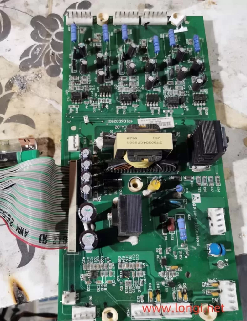
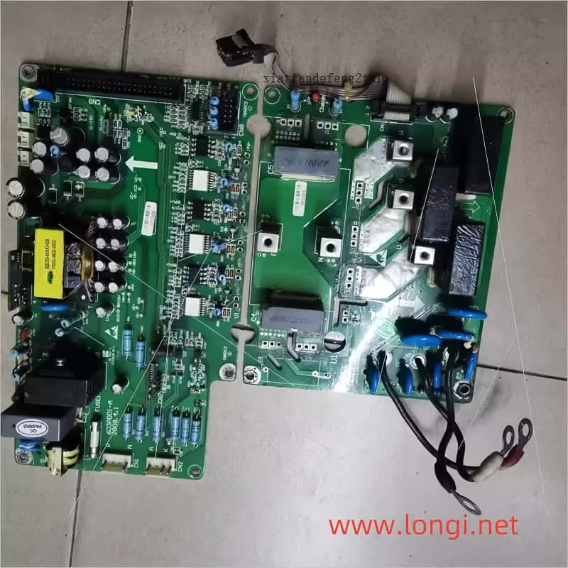
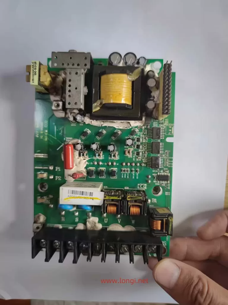
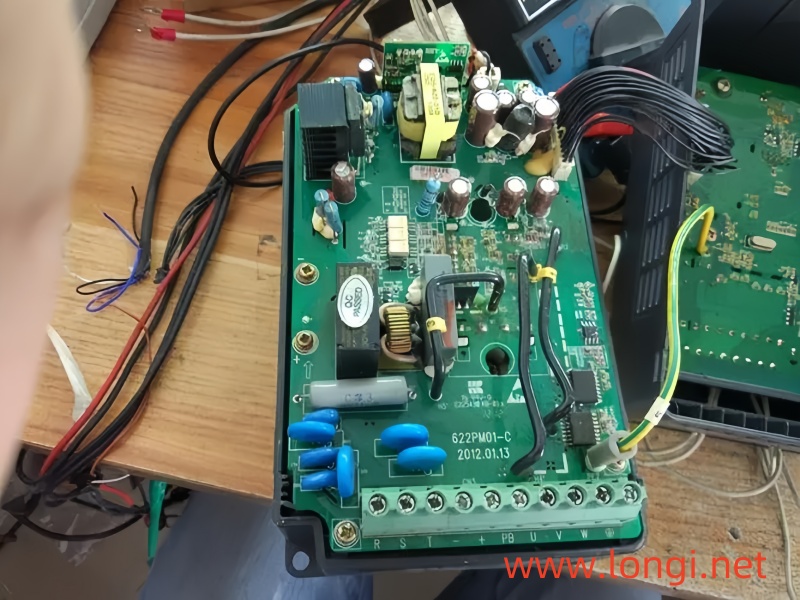
Cause: A cement plant user sent a 75kW micro energy WIN-G9 frequency converter for repair. The cause of the malfunction was that during operation, the frequency converter suddenly caught fire and emitted smoke, causing it to shut down. Upon inspection, the power input circuit of the machine is a three-phase half controlled bridge. Using its controllable rectification principle, the DC main circuit energy storage capacitor is “soft charged”, eliminating the commonly used charging contactor for low-power frequency converters. In fact, the semi controlled bridge here is equivalent to a contactless soft switch. Upon inspection, it was found that there were obvious signs of arc flashover and burning on the terminals of one of the thyristor modules, but the measurement did not indicate a short circuit. During disassembly, it was found that the fixing nut was easily removed, and the cause of the flashover seems to be due to loose connection screws, causing poor contact. This module is a combination of a diode and a unidirectional thyristor. Further check the control board and inverter main circuit, and there are no abnormalities. After removing the module, the remaining two phase half control bridges were used as power inputs. After being powered on, a 2.2kW low-power three-phase motor was tested and there were no issues. After replacing it with a new module of the same model, it was installed on site.

To be cautious, first adjust the operating frequency to 5Hz, and the frequency converter is loaded with a fan. First, disconnect the motor connector and let the motor run at no load. This trial run was a shock! When the frequency is below 5Hz, the no-load operating current is 45A. Although it feels slightly higher, it may be caused by the repair of the motor winding or the adjustment of the parameters of the frequency converter, such as the starting curve or torque compensation, which was not taken into consideration. When the speed was increased to 10Hz, both the current displayed on the frequency converter panel and the output current measured with a clamp meter reached 100A! And the oscillation amplitude of the output current is very large, but when measuring the three-phase output voltage, it is about 70V, balanced and stable. Disconnect the motor connection wire and power on to measure the output of the frequency converter. The output voltage is 70V at 10Hz, 150V at 20Hz, and 250V at 35Hz. As the operating frequency increases, it reaches 400V at 50Hz. During this process, the balance of measuring the three-phase output voltage is very good. The V/F curve output by the frequency converter conforms to the quadratic load torque characteristics. No problem. The output voltage is balanced and stable, while excessive output current and severe current fluctuations are clearly caused by abnormal loads. This is a conclusion drawn from conventional judgment.
Discuss with the relevant technical personnel of the factory, attempting to identify the reasons for the motor and mechanical aspects. For example, whether the motor is newly repaired or whether the winding is poorly wound; Check for wear and unstable operation of bearings; Is there any looseness or non concentricity in the connecting shaft; The wind blades have deformation, etc. Restore the wiring of the original power frequency starting cabinet, compare the power frequency starting motors, and eliminate the above doubts one by one. According to on-site observations, the motor and connected loads are in good condition, and there is almost no electrical and mechanical noise during operation. The no-load current under full speed operation is only less than 35A, with three-phase balance and no fluctuation! There is no problem with the motor and load, and the problem is still with the frequency converter.
So where is the fault location of the frequency converter? It’s a bit scratching my head. Is the current detection inaccurate, causing erroneous output? The current value displayed on the observation panel is close to the value measured by the clamp ammeter, and there should be no problem. Is there still a problem with the CPU motherboard and the output driver waveform incorrect? It doesn’t make sense. All digital circuits, why is the waveform incorrect?
Fortunately, there is another inverter of the same model and power not far from here on site, carrying the same load. That’s great. This has brought great convenience to comparative experiments. The factory was eager to start the machine and provided active cooperation. Swapping the current transformers of two frequency converters is ineffective; Swapping the CPU motherboards of two machines is invalid. Retrieve the DC voltage display of the main circuit, which is 550V, and there is no problem with the voltage sampling circuit. I can no longer figure out which circuit the problem lies in. When the comparison machine is under load, the operating current is 75A at 10Hz. When it reaches 35Hz or above, the operating current only reaches 100A, which is smaller than the current of this motor with no load. The no-load current is much higher than the load current, so there must be a problem with the frequency converter.

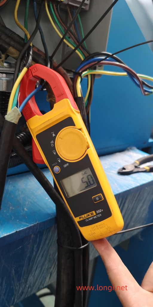
During the trial operation, I occasionally measured the three-phase output current of the inverter using a current clamp meter, and even discovered an incredible phenomenon! The input and output currents of this frequency converter are completely disproportionate, with a difference of more than 10 times!
When outputting a 40A current, the input current is a few amperes, which is almost undetectable; When outputting 100A current, the input current is only below 8A! Strange, it doesn’t comply with the law of conservation of energy. Where did the 100A output current come from?! It’s like an airtight water pipe, where 1 cubic meter of water enters and 10 cubic meters of water flows out. The water inside the pipe cannot come out.
We all know that in general, the input current of the frequency converter is always smaller than the output current. The reason is that the energy storage capacitor in the DC circuit acts as if a reactive power compensation cabinet is installed at the motor end. When the frequency converter is unloaded or lightly loaded, a portion of the current is provided by the energy storage capacitor to the load, reducing the current absorbed by the frequency converter from the grid. As the load increases, the input current of the frequency converter increases proportionally. When the rated load is applied, the input current and output current of the frequency converter should be close to equal. When outputting 40A, the input is only a few amperes; When outputting 100A, the input current has reached 70A; When the output current reaches 140A, the input current has also reached this value. Under normal circumstances, there may be a difference in input and output currents, but there will not be an extremely significant difference as mentioned above. The huge difference made me doubt whether the measuring instrument was broken. After changing the watch and retesting, the same result was still obtained.
There’s no way out. Consult the manufacturer. Due to the urgent need to solve the problem and find the answer, it’s not worth considering whether long-distance phone calls are expensive at this time. The technical personnel from the frequency converter manufacturer replied that this model of frequency converter is the earliest produced frequency converter, and there are problems with slightly higher no-load current and current fluctuations, but it is a normal phenomenon and does not affect its use. After being loaded, the current will stabilize. It is best to connect a motor of the same power for testing to see if there is a problem with the motor or load. Problems with motor bearings. If all motor and load issues are eliminated, as long as the three-phase voltage output of the frequency converter is balanced and the output current does not exceed the rated current of the frequency converter, can the machine be tested under no load or on load. Can’t it break down. As for the proportion of input and output currents, it is difficult to have a fixed proportion due to different load conditions. It’s not proportional. Don’t get entangled with the issue of proportion.
Think about it too. As long as the output three-phase voltage is balanced and does not exceed the rated current, can the load test be conducted. Can’t the frequency converter break down. Perhaps after being loaded, there will be no significant fluctuations in the output current. Maybe it’s normal.
We had to conduct a load test and a miracle occurred (which was surprising): when operating at 10 Hz and outputting a current of 40A, the output current was only 7 out of 8 amperes. When operating at 30 Hz, the output current is 60A and the input current is 25A; When operating at 40 Hz, when outputting a current of 100A, the input current is 70 amperes. The operating current has decreased and the fluctuation has decreased, and it is basically stable. The three-phase voltage and three-phase current are both balanced and relatively stable. The problem was inexplicably solved.
Thank you to the manufacturer’s technical personnel for their guidance: why not try the machine on load. But due to encountering this situation for the first time, abnormal current occurs at no load, and it is not dare to increase to full speed for operation. I’m even more afraid to carry it. I always want to find out the reason before loading. I always thought this was an abnormality with the frequency converter.
After the frequency converter was put into operation and returned from the site, I am still pondering this issue.
Remembering the problem of high zero line current in a power plant during maintenance, caused by harmonic components in the transmission line. It’s harmonic current. Is there also a significant harmonic component in the output circuit of the frequency converter during no-load or light load operation? Where does this harmonic component come from? Is the measured result true?

The analysis shows that there are significant harmonic components in the output current during no-load operation. There may be two reasons for the high harmonic current: 1. The output PWM wave of the inverter is not ideal enough, and the modulation method is not optimal. The software control concept has not been optimized (the new machine must have been improved); 2. When unloaded, it is equivalent to a serious mismatch between the power supply capacity and the load capacity. The power supply capacity is much larger than the frequency converter capacity, which is also a major reason for the generation of harmonic currents. When running on load, the capacity matching situation improves, and the harmonic components are greatly reduced. The combination of these two reasons has stumped me, an old electrician. For me, during the test drive, I made an empirical mistake. I was bound by the ratio of input and output currents and almost surrendered.

Posted on Leave a comment

Three Examples of IGBT Module and Driver Fault Frequency Converter Maintenance Process

A. One Dongyuan 7300PA3.7kW frequency converter was sent for repair. The power was connected and it was detected that there was output in the U, V, and W phases, but there was severe phase deviation. It was determined that the drive circuit was abnormal or the module was damaged. Measure the open circuit of the upper arm diode inside the U-phase power stage of the inverter circuit. In general, the IGBT transistor connected in parallel with this diode is also often damaged. In fact, the IGBT tubes were first burnt out by short-circuit current, and the parallel diodes were also damaged by the impact.

After removing the inverter module SPIi12E, all the pins of the inverter module are empty, and the six drive circuits are ready to be tested when powered on. Once powered on, the frequency converter experiences an overheating fault, and the CPU locks the output of the drive pulse in the fault state. Due to the absence of trigger pulse output, it is impossible to detect the quality of the driving circuit. The locking state of the overheating fault must be temporarily released before checking the quality of the drive circuit.
Observe that the inverter module on the circuit board has two terminals labeled T1 and T2, which may be the internal overheat alarm output terminals of the module. One end is led into a 5V power supply through a resistor, and the other end is grounded. When this terminal is suspended, T1 terminal outputs a high-level module overheating signal through an pull-up resistor to protect the shutdown. After short circuiting the T1 and T2 terminals, there will be no protective shutdown when power is supplied.
Check that there is no trigger pulse output in the IGBT drive circuit of the U-phase upper arm. After replacing the drive circuit IC/PC923, the six pulse outputs are normal.
After replacing the IGTB inverter module with a new one, remove the short circuit of the T1 and T2 terminals, and conduct a power test to ensure normal operation. Experience has shown that when an IGBT tube is damaged, the corresponding drive IC will also be damaged due to impact. It is also necessary to inspect the drive IC of the same branch of the damaged module and not hastily replace it with a new module to avoid causing damage to the new module again due to abnormal drive circuit!
B. An Alpha 18.5kW frequency converter with six single tube IGBT tubes (modules) forming a three-phase output circuit, one of which is damaged. CPU motherboard jumps 2501, panel operation fails. The cause of the malfunction of the machine was damage caused by lightning strikes.

The operation panel shows 2501 when powered on, and all operations are malfunctioning. CPU motherboard malfunction, caused by damage to the CPU and peripheral communication circuits. Let’s not worry about it for now. First, fix the driver board before proceeding.
Check the driving circuit, a total of six A316J chips are responsible for six driving pulse output tasks. Three drive circuits that output upper arm pulses are damaged, but there are no integrated circuits of the same model available for replacement. Based on the experience of repairing other brands of frequency converters, using only three A316J chips (used for three-phase lower arm drive) as the three-phase OC signal alarm output can meet the protection requirements. Therefore, the other three pieces were replaced with 3120 (same as PL250V) to drive the optocoupler IC. The original IC was packaged in a 16 pin dual row SMT package, and the replaced IC was packaged in an 8-pin dual row inline package. But the connection is also relatively convenient. Only weld the 8 pins of the new IC to the original 12/13 pins, weld the 5 pins of the new IC to the original 9/10 pins, and connect the 6/7 pins of the new IC to the original 11 pins; Due to the original IC input method being an operational amplifier input and the new IC being a photoelectric tube input, a larger input current is required. Remove the 202 grounding resistor from the original input side and replace it with a 5.1k resistor. Connect the 3 pins of the new IC to ground, and connect the original 1 pin in series with a 300 ohm resistor to the 2 pins of the new IC. Power on and test, and the static voltage is normal.
At this point, after replacing the CPU motherboard with a new one, the static output negative pressure and dynamic pulse output of the six drive circuits were tested to be normal upon power on. After replacing the damaged IGBT module, the machine was tested normally.

C. A 7.5kW frequency converter has been reported by the user as having no major issues, but it has output but cannot operate due to phase deviation. Check if there is an abnormality in one of the six driving circuits. The driving IC model is PC929 (or A4503?). Measure that there are no pulse outputs on the input and output sides of the driving IC. The input side of the IC is directly connected to the pulse output terminal of the CPU. Suspecting a faulty internal pin circuit of the CPU, the PC929 input terminal was disconnected. The voltage at the CPU pulse output terminal increased, but as soon as the driver IC was connected, it dropped to nearly 0V.
Analysis: Due to the direct output of the CPU driving the photoelectric tube, it needs to output a large current. Long term operation may cause aging and failure of the output stage or other faults, resulting in an increase in output internal resistance. When unloaded, there is a certain amplitude of voltage signal, but once connected to the load, even if the signal voltage drops significantly. Replacing the CPU motherboard for this malfunction is a quick solution. One reason is that the maintenance cost is high, and the other reason is that it still needs to be purchased externally, and the repair time required by the user is very tight. Isn’t there a better way? Based on the above analysis, although the pulse output pin of the CPU has aging and failure phenomena, which greatly reduces its load capacity, assuming that its signal current is not used and only its output voltage signal is used, this defect can still be remedied to achieve the purpose of repair. By passing the CPU pin through an external amplifier stage, the signal voltage should meet the requirements for driving the photodiode (PC929 input side photodiode).
Measure that both pins on the input side are 5V high level, and the pin connected to the CPU is a negative pulse input. If you have a PNP transistor on hand, connecting one transistor and a 5k resistor should be able to complete the task. But I only have NPN type transistors on hand, which can only be achieved by using two inverters. Disconnect one pin of the driver IC from the CPU output, connect the copper foil strip to a 50k resistor, and then connect the base of the transistor. Connect the collector in series to the base of the next transistor, and then connect it to+15V through a 10k resistor. Ground the two emitters and connect the lower collector to the disconnect pin of the driver IC. Power on test machine, six pulse outputs are normal. Restore the power supply to the inverter module, and the three-phase voltage output is normal.
The CPU of this machine is damaged and faulty. After using two resistors and two transistors, the problem was resolved and successfully repaired.

Posted on Leave a comment

Repair process of TECO 7200GA-22kW VSD after lightning strike

Received a 7200GA-41kVA frequency converter for repair, which is a lightning fault. After replacing the damaged input rectifier module, switch tube, and shunt tube of the switching power supply, the operation panel screen displayed normally, indicating that the problem is not significant.

The negative pressure and optocoupler drive input signals of the six channels were tested to be “normal”. During the assembly test of the whole machine, the OC jumped immediately upon power on, but the operation could be started after resetting. The screen frequency output was normal, but there was no three-phase voltage output at the U, V, and W terminals during the actual test. The local driving IC adopts optocouplers PC923 and PC929, which cooperate with SN0357 to return OC signals.
Check the power amplifier circuit on the output side of the driving IC and the detection circuit of the IGBT tube, and there are no abnormalities. When testing the pulse input pin of PC923, it doesn’t feel right. Why is the level of pin 3 high and pin 2 low? Is it because the driver power supply is reversed? 2. Three pins are the input circuit of the photodiode, two pins are the anode of the photodiode, and three pins are the cathode of the photodiode. According to common sense, the two pins are usually powered by+5V and then stabilized to provide an excitation power of about 4V, while the three pins are connected to the pulse output terminal of the CPU. Low level output is effective, that is, when outputting, current is pulled in from the three pins of PC923 to make the diode conductive. When there is a trigger pulse input and the frequency is low, the voltage of pin 3 oscillates up and down to 3V. As the frequency increases, the voltage of pin 3 gradually stabilizes at around 3V. When there is no output, pin 3 is a high level of around 4V (equal to the level value of pin 2).
The current detection results are as follows: when no running command is input, pin 3 is a high level of 0.5V, and pin 2 is a low level close to 0V; When entering the run command, pin 3 drops to 0.2V and there is a change in high and low levels, indicating that the CPU pulse has reached PC923. At the beginning of the maintenance, I took a detour and only paid attention to the changes in high and low levels, without paying attention to the magnitude of the voltage value. Obviously, the loss of 2-pin power supply voltage prevents the IGBT transistor from receiving excitation pulses, resulting in no output voltage from the frequency converter.
Check that the 2-pin power supply is a simple series connected voltage regulator with a transistor and a voltage regulator. The base bias resistance of the transistor is open, causing the supply voltage to be zero. After replacing the bias resistor, measure the voltage on pins 2 and 3 of PC923 to return to normal. After receiving the operation command, the frequency converter has output from the U, V, and W terminals.
Further investigate the reason for the OC jump upon power on. Measure the SN0357 optocoupler device that transmits the OC signal, and the voltage value of the two pins on the input side is zero, indicating that it did not input the OC signal. However, measure the voltage value of the two pins on the output side of the three optocouplers to be 0.5V! But since there is no OC signal input, the voltage between the two pins should be 5V (one pin is connected to a 5V ground level), and there is only one possibility, that is, the 5V pull-up resistance of the signal output pin has changed or is open circuit. At this point, the CPU mistakenly believes that it has received the OC signal returned by the drive circuit, and therefore gives an alarm. Try connecting a 10k resistor between the signal output pin and the 5V power supply. Start up and test the signal output pin to be 5V. Repeat the power supply several times and no longer experience OC faults.

The above two faults actually come from one reason: power loss. The input pin of the pulse signal and the output pin of the OC signal are both directly connected to the CPU pin. When the pull-up high level disappears, the CPU pin only has a low level of 0.5V left. This level is not enough to drive the optocoupler to send out the trigger signal of the inverter module, and it also leads to the detection of low levels and the jumping of the OC fault code when powered on. And 0.5V is also the critical level for detecting signals such as OC, so after performing a reset operation, it can start running again.
Note:
The motherboards of various series of Dongyuan frequency converters have good replacement characteristics, and after replacement, only the corresponding capacity value of the frequency converter needs to be readjusted. After changing its capacity value, the relevant parameters for checking the rated current value of the motor are also automatically modified.
The capacity labeling of Dongyuan frequency converters is mostly not based on kW, but on kVA. For example, for a 22kW capacity, it is labeled as 41kVA with a rated current of around 48A. In the relevant manual, the capacity is set by comparing the HP horsepower with the rated current. Moreover, the setting of horsepower size is not simply expressed in numerical terms, but also mixed with English letters to indicate the size of horsepower value (actually using hexadecimal notation). When initially adjusting its capacity value, it is often difficult for Master Zhang Er to understand and adjust it, and the parameters cannot be written in.
The corresponding relationship between kW, KVA, and HP values is not clear to most users. I don’t know what the Dongyuan people were thinking about doing this. 1HP=0.75kW, indicating that the horsepower is less than the kW value; KW is the active power value, which can be approximated as the actual power value. That is, a 22kW frequency converter can drive a 22kW motor, and the power capacity is sufficient; And kVA is the apparent power value, which means that when there is such power, but it drives some loads such as motors/inductive loads, it cannot reach the marked output value because the motor load requires reactive power consumption, and kVA is the sum of active power and reactive power. The kVA value is virtual (not discussed here) and can be selected based on the rated current value.

The comparison table between the motor capacity HP and the set value is as follows:
HP: Set value:
25 (18.5kW) 29
30 (22kW) 2A
40 (30kW) 2B
50 (37kW) 2C
60 (45kW) 2D
75 (55kW) 2E
100 (75kW) 2F
125 (90kW) 30
150 (110kW) 31
175 (130kW) 32
215 (160kW) 33

Posted on Leave a comment

Repair of Switch Power Supply Fault in TECO 7200GA-30kW Inverter

After being damaged and repaired by lightning strikes, the frequency converter has been running for over a month and has experienced strange malfunctions: there is a random shutdown phenomenon during operation, which may occur every few days or every few hours; Difficulty starting, capacitor charging short circuit contactor jumping during the starting process, starting failed, but the operation panel does not display a fault code. After successfully starting with some effort, it can run for a period of time again.

Remove the control board from the site and short circuit the terminals of the thermal relay to prevent it from entering the thermal protection state and unable to test the machine; Short circuit the contact detection terminal of the capacitor charging contactor to prevent it from entering a low voltage protection state. The machine cannot be tested, and a comprehensive inspection was conducted. No abnormalities were found during the inspection, all of which are good.
Install the control board back into the machine, power on and test the machine. When starting, the contactor jumps and cannot start. After unplugging the connection of the 12CN plug cooling fan, the situation greatly improved and the success rate of starting increased. Upon careful observation, the brightness of the display panel decreased during the startup process, indicating that the fault was due to poor load capacity of the control power supply.
When each power supply output is unloaded, the output voltage is normal. Connect resistive loads to the output of each power source, and slightly reduce the voltage value+ After 24V is connected to the cooling fan and relay load,+5V drops to+4.7V, and the screen display and other operations are normal at this time. But if the frequency converter is put into the startup state, the relay will jump, and occasionally fault codes such as “low DC voltage” and “communication interruption between CPU and operation panel” will appear, causing the operation to fail. In measurement, when+5V drops below+4.5V, the frequency converter will immediately change from starting state to standby state. Detailed inspection of the load circuits of each power supply shows no abnormalities.
Analysis: The judgment of poor load capacity of the control power supply is correct. Due to the strict requirements of the CPU for power supply, it can still barely work at no less than 4.7V; But when it is below 4.5V, it is forced to enter “standby mode”; When the voltage is between 4.7V and 4.5V, a fault alarm will be issued to detect the operation of the circuit.
But unexpectedly, the maintenance of this malfunction was quite tricky, and after checking all the relevant components of the switch power supply, none of them were damaged! Helpless, I attempted to conduct a parallel resistance test on R1 (5101), one of the reference voltage divider resistors of U1 (KA431AZ), with the aim of changing the divider value to increase the output voltage. The measured output voltage has slightly increased, but the load capacity is still poor. Upon closer inspection of the circuit board, it appears that there are welding marks on the diversion adjustment tube Q1, but it appears that its model is the original one. Even if it is replaced, it will still be removed and replaced from similar machines. The switch transistor Q2 of this machine is a bipolar transistor with high back pressure and high amplification, which is difficult to purchase in the market, and the circuit has strict requirements for the parameters of these two transistors. Combined with fault analysis, the working point of the shunt adjustment tube is offset, causing too strong a shunt on the Q2 base current, which will result in poor load capacity of the power supply. Try to connect a resistor R6 (330 ohms) in series with a voltage feedback optocoupler and a 47 ohm resistor to reduce the base current of Q1, thereby reducing its shunt ability towards Q2 and enhancing the load capacity of the power supply. Power on test machine, regardless of loading or starting operation,+5V stable output 5V, troubleshooting!

Fault inference: The Q1 switch tube has aging phenomenon and the amplification ability has decreased. Therefore, the insufficient Ib value after shunt makes it fully conductive (increasing the conduction resistance), resulting in a decrease in the power supply’s carrying capacity; There is a characteristic deviation phenomenon in the shunt branch, which leads to excessive shunt and poor driving of the switching tube, resulting in poor load carrying capacity of the power supply.