Posted on Leave a comment

616G3-55kW Yaskawa inverter main circuit diagram and inverter maintenance ideas

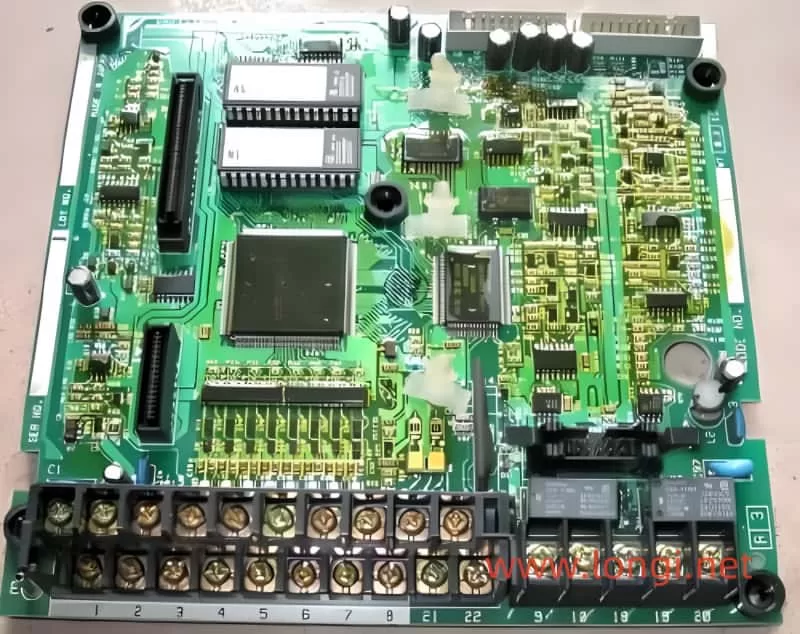
1. Main circuit of “616G3-55kW Yaskawa inverter”

The structures of the main circuits of all inverters are similar or even identical. The main circuits of Yaskawa inverters and Taiwan Teco inverters are exactly the same. Later I observed that the control panels of the two machines are the same, and the control panel and parameter settings are also similar. It is found that the two machines are similar or even identical from hardware to software, which will bring a lot of convenience to installation, debugging and maintenance. As long as there is a technical data reference at hand, you can debug and repair the two devices.

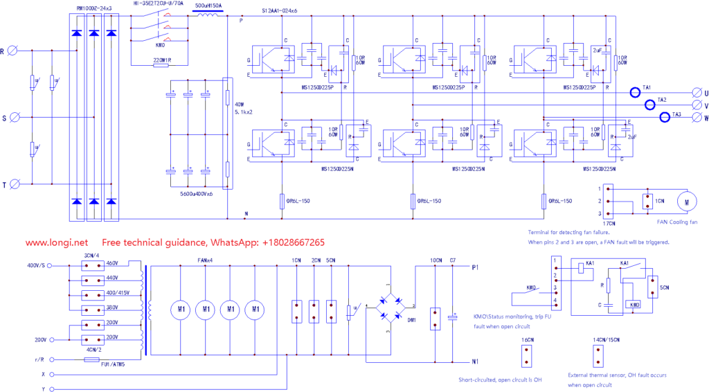
When we open the shells of these two high-power inverters and check the main circuits, the six large rectangular box-shaped objects installed above the inverter modules (in parallel with the modules) will first arouse our interest – the model number MS1250D225P is connected in parallel with the upper arm IGBT tube of each phase, and the model number MS1250D225N is connected in parallel with the lower arm IGBT tube. To use a phrase from the Internet: What on earth is this? What is the purpose of installing it here?

Generally speaking, anything connected in parallel to the IGBT tube, whether it is a capacitor or a resistor-capacitor network, is set up to protect the IGBT tube. That is, when the tube is cut off, the energy formed by the reverse voltage is quickly consumed, providing a reverse current path to protect the IGBT tube from (in fact, it makes it bear less) the impact of reverse voltage. As we all know, whether it is a bipolar or field effect device, there is often a certain amount of surplus in the forward voltage, but the ability to withstand reverse voltage is extremely fragile. Therefore, the things connected in parallel to the IGBT tube can be said to complete this task of consuming reverse voltage.

It should be noted that the internal circuits of MS1250D225P and MS1250D225N were not opened for verification. After the module was damaged, these two devices were often intact, so it was not convenient to disassemble them after they were damaged. The internal circuit in the above figure was drawn based on measurement and speculation, and is only a reference for readers. I have searched a lot of information and searched on the Internet, but I have not found any information about this component. It is obviously easy to mislead to analyze the principle based on the speculation of the circuit. Therefore, the analysis of its principle is temporarily omitted.

However, after connecting such components in parallel to the module, it will bring us new experience in maintenance. See below.

According to the conventional maintenance method, after replacing the damaged module, before conducting the power-on test, we must cut off the P point in the above figure, connect two 25W (or 40W) bulbs in series, and then power on. In this way, if the inverter module circuit or drive circuit is abnormal, causing the two IGBT tubes of the upper and lower arms to short-circuit the DC power supply, the expensive IGBT module will not be damaged due to the current limiting effect of the bulb. Other brands of inverters connect small-capacity capacitors of the picofarad level in parallel at both ends of the tube. After powering on or starting the inverter, as long as the U, V, and W output terminals are unloaded, the bulb will not light up. But the performance of Yaskawa inverters in maintenance is different. Connect a bulb in series at point P, power on, and the bulb does not light up. It is correct, I breathed a sigh of relief; press the operation panel to start the inverter, and the bulb becomes bright! It is broken, the output module has a short circuit! This is my first judgment. Check the module and drive circuit during power outage, and there is no abnormality. Looking back at the circuit structure, after removing the MS1250D225P and MS1250D225N, the light bulb did not light up after starting the inverter. The three-phase voltage of the no-load output was normal. These two components and the external 10 Ω 80W resistor provided a current path of about 100 mA, making the 25W bulb bright. Sacrificing tens of watts of power consumption in exchange for higher safety of the IGBT tube is the characteristic of the module protection circuit of the Yaskawa inverter.

After the inverter is started without load, due to the relationship between components such as MS1250D225P and MS1250D225N, the inverter circuit itself forms a certain circuit path, which is not caused by the inverter module failure. This machine is a special case. The existence of a circuit path does not necessarily mean that the module is damaged. Observe which components provide the current path? When fresh experience solidifies into a fixed mindset, misjudgment of faults is inevitable.

The control power of the whole machine is obtained from a multi-tap transformer at the bottom of the figure. The short-circuit wires of sockets 3CN and 4CN are different, and the level of input voltage can be adjusted to ensure the accuracy of the secondary winding AC220V voltage. The cooling fan uses an AC220V power supply, which is filtered and used as the input of the switching power supply. When repairing the driver board alone, the terminals 2 and 3 of the fan; 3 and 4 of the contactor terminals; 14CN, 15CN, and 16CN must be short-circuited, and fault signals such as undervoltage (FU/LU), overheating (OH), and fan failure (FAN) must be manually eliminated, so that the CPU can output six pulse signals, which is convenient for checking the drive circuit.

2. Drive/protection circuit of “616G3-55kW Yaskawa inverter”

“616G3-55kW Yaskawa Inverter” drive circuit/protection circuit diagram

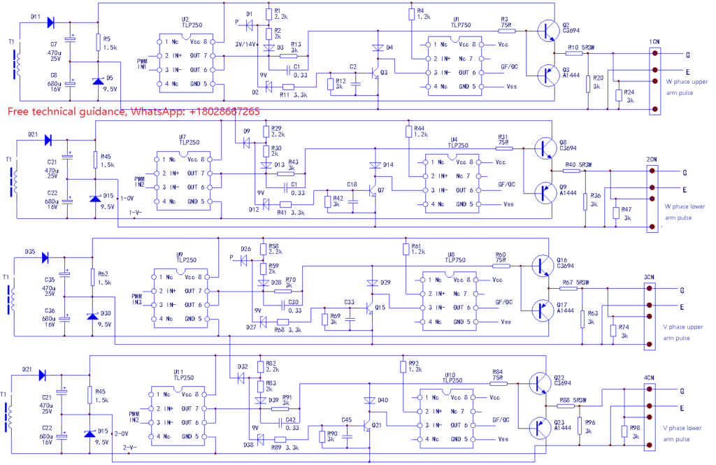
The types of drive circuits are similar. The most common ones we see are drive detection circuit (protection circuit) is also integrated. Although you can find circuit information about A3316J, etc., and you can see the internal unit block circuit diagram and the introduction of the circuit principle, you always feel a little confused about the specific composition of its protection circuit – the protection circuit inside the IC is indeed invisible and intangible. It happens that this circuit is a detection and protection circuits composed of ICs such as PC929 and A316J, in which the module fault circuit composed of discrete components, which makes it easier to understand the detection and protection action process. Slightly redrawing the pulse and protection circuit in the above figure, you can see how the IGBT tube voltage drop detection circuit implements the protection action on the module:

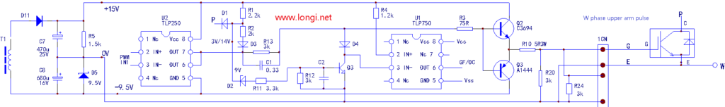
Circuit principle: The PWM pulse signal from the CPU pin is isolated and amplified by the U2 optocoupler and then sent to the module protection circuit. Under normal conditions, this pulse signal is amplified by the push-pull power amplifier circuit of Q2 and Q3 to directly drive the IGBT module. It is generally believed that the IGBT module is a voltage-type drive module, which is biased. The input gate-emitter junction capacitance of the IGBT tube just needs a transient large inrush current! This is why Q2 and Q3 are used for power amplification. The introduction resistor of the drive signal is also a 5 Ω 8W power resistor. In this sense, in essence, the IGBT module is still a current-type drive device. This is the author’s opinion, is it correct? When the current output capacity of the drive circuit is insufficient, the three-phase output current will be intermittent, the motor will vibrate, and a rumbling sound will be emitted. The principle of the pulse processing circuit can be found in other figures. The focus here is on how the protection circuit works.

When the inverter does not receive the start signal, the output pins 7 and 8 of U2 are cut-off negative voltages. If the 0V power line is used as the reference point, the voltage of pins 7 and 8 is about -9.5V (ignoring the saturation voltage drop of the internal tube). This negative voltage is introduced to the base of Q2 and Q3 through R13 and R3. Q2 is cut off due to reverse bias, Q3 is turned on due to positive bias, and the gate bias of the IGBT module is negative and is in the cut-off state. Resistors R1 and R2 divide +15V and negative -9.5V to obtain a 3V level. D9 is a voltage regulator with a breakdown voltage value of 9V. The voltage division value of R1 and R2 is not enough to cause it to break down, so Q3 has no bias current and is in the cut-off state. There is no input current to the photocoupler U1, so no fault signals such as GF (grounding) and OC (overload, short circuit) are returned to the CPU. When the CPU sends a drive pulse, the 7th and 8th pins of U2 become positive pulse voltages with a peak value of 15V, and the positive pole of D1 rises to +15V at this time. At this time,two situations occur: In one case, the module is good, and the IGBT tube is quickly turned on under the drive of the positive excitation pulse. It can be considered that the P and E points are short-circuited instantly. The negative terminal potential of D1 is instantly pulled to 0V, and the negative terminal potential of D2 is also pulled to below 1V. Because it does not reach the breakdown value of D2, Q3 still has no base bias current and is cut off; In another case, the module has caused the operating current to be too large due to abnormal load, or the IGBT tube is not turned on well due to the poor driving circuit itself such as Q3. The negative terminal of D1 is high potential and is cut off, and +15V causes D2 to break down through R1, Q3 is biased and turned on, and the positive pulse voltage of the base of Q2 is pulled to zero level, and the IGBT module loses the pulse and is cut off. At the same time, the conduction of Q3 generates the input current of U1, and U1 sends the module fault signal to the CPU. It can be seen that the protection circuit of this circuit first cuts off the driving pulse of the IGBT tube and sends out the module fault signal at the same time. The protection is timely and fast.

3. Drive/FU circuit of 616G3-55kW Yaskawa inverter

“616G3-55kW Yaskawa Inverter” Drive/FU Circuit Diagram

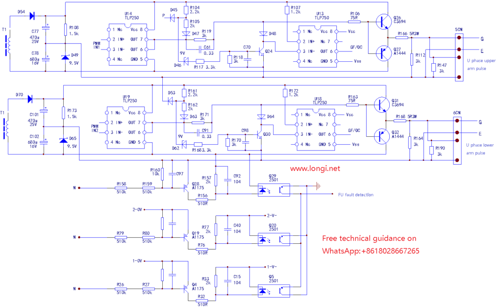
The protection circuit of the drive circuit implements protection actions and sends OC signals according to the tube voltage drop of the IGBT tube during the sending of the excitation pulse. According to the information, the on-state voltage drop of the IGBT module is about 3V under normal (rated current) conditions. When the tube voltage drop reaches 7V or more, it means that the current flowing through the IGBT module has exceeded 180% to 200% of Ie. At this time, the protection action is of course the faster the better. The purpose of setting up this protection circuit is to make up for the slow protection action of the subsequent current detection circuit such as the current transformer. The current detection circuit inevitably uses a large capacity filter capacitor, which makes the circuit have a certain time constant and slow response. The tube voltage drop detection circuit of the IGBT can be called a fast protection action circuit because of its rapid response, just like a fast action unit, which is used to deal with emergency events. The treatment of slight overcurrent and current limiting regulation is still implemented by the current detection circuit of the current transformer circuit.

The drive circuit is also equipped with a fuse detection circuit. In general, a fast-blow fuse is connected in series at the P end of the DC circuit to implement module protection. However, this machine circuit has a fuse connected in series at each phase output module. The inverters produced by each manufacturer generally have the following trends: early products are inevitably crude, old and heavy, and their user control functions are not perfect, but there is a large margin in their production and selection of materials; they are conservative in protection performance, but they do not hesitate to add components that seem redundant now to ensure the reliability of the protection circuit. The early products of Yaskawa inverters were no exception. With the advancement of product technology and the fierce market competition, the functions of inverters have been improved, while the costs have been reduced, and there is even a suspicion of cutting corners. The operating reliability of inverters has also been compromised, and domestic inverters should take this as a warning.

The detection circuit of the three-way fuse blown is to compare the 0V line of the lower three-arm drive power supply with the N line of the main DC circuit to determine whether the fuse is normal. Under normal conditions, the 0V line and the N line of the drive power supply are connected through the fuse and are of equal potential. That is, the E pole of the lower three-arm IGBT tube is connected to the N line of the main DC circuit. Therefore, the base bias of the transistors Q4, Q19, and Q28 is zero. All three tubes are cut off. When the fuse of any phase output module is disconnected, the N line and the 0V line of the phase drive power supply produce a huge potential difference, and the transistor is turned on by positive bias. The three optical couplers Q5, Q20, and Q29 are connected into an OR gate circuit. The input signal of any optical coupler will be transmitted to the same output point, and the fuse signal of the fast insurance will be transmitted to the CPU, so that the CPU reports the FU (fuse) broken signal and refuses to accept the start signal.

There is also an interesting problem of the order of fault signal alarm of Yaskawa inverter. For example, when the power is on, a warning of the fault code is given for overheating, undervoltage, overcurrent, fan failure, fuse failure, etc., and the startup operation is refused; during the startup, the module fault detected by the module protection circuit is warned with the GF (ground fault) code. When the module fault is detected during operation, the OC (operating overcurrent, load short circuit, etc.) fault code signal is reported. The same signal output by the IGBT tube voltage drop detection circuit is output at different times (one is during the startup process, and the other is during the operation process), but the inverter reports two different fault codes (GF: ground fault; OC: overload or short circuit fault). Similarly, in the current and voltage detection circuits, the same means are sometimes used. The overcurrent or overvoltage signal reported by the same protection circuit may report different fault codes or take different treatment measures due to the different working states of the inverter (starting or running). All this depends on the ideas of the software designer. The control ideas of each manufacturer’s inverter must be similar. Pay attention to the relevant characteristics of the inverter fault alarm to facilitate efficient diagnosis of the fault.

When analyzing the protection circuit, you need to look at the main circuit and the drive (protection) circuit in two or three parts. Many drawings are broken down into individual unit circuits. Readers must strengthen their ability to read drawings in a comprehensive and coherent manner. This is a piece of advice I give you.

Posted on Leave a comment

Is it necessary to replace the board to repair the GF fault reported by Yaskawa VSD?

Recently, an Yaskawa 616G3 55kW frequency converter was repaired, and when it was powered on, it reported a GF – ground fault. The maintenance process was full of ups and downs, which was quite troublesome. I have also searched on some websites for analysis of this fault, and many posts have reported that this fault is quite stubborn and requires a replacement board to be repaired. Replace the motherboard or driver board? Not explained clearly. Due to the deadlock in the maintenance process, I almost agree with this statement.

But looking at the structure of the protection circuit of the Yaskawa frequency converter, it is actually the same as other frequency converters. The fault signals of overcurrent OL1, OL2, and OL3 should be reported by the current transformer and subsequent current detection and processing circuit to the CPU; The GF (ground) and OC (load side short circuit) fault signals should be directly fed to the CPU by the protection circuit of the driving circuit board. The difference is that in the initial startup stage, the detection module is abnormal, that is, it reports a GF fault. If the module is detected to be abnormal during operation, an OC fault will be reported. These two signals actually reveal a kind of information: in the initial stage of startup, the three-phase output voltage has not been established yet, and the load has not yet run. The source of the fault at this time should be the abnormal drive circuit of the frequency converter or the IBGT module itself; If there is an abnormally high current during operation and the OC jumps, the probability of load side failure is high. The difference and indication between GF and OC faults do make sense.
The possibility of GF failure reporting upon power on due to CPU damage is extremely small. And GF malfunction is definitely reported directly to the CPU by the driving circuit. Replacing the board seems like the only option is to replace the driver board. Replacing the CPU motherboard to fix this fault does not meet the logical conditions. This is purely a hardware circuit (protection circuit) malfunction. If we don’t expose it completely, I don’t think I would be willing to accept it.
The original fault of the machine was that two of the three-phase power input rectifier modules were damaged, and two of the six inverter IGBT modules were damaged. The driver board was impacted by damaged modules, and some components were also damaged. This machine was left unused for two to three years for some reason before coming to my repair department for repairs. We first checked the main circuit, checked the modules and capacitors, and inquired about the source and price of the damaged modules. Then prepare to purchase the module for repair after repairing the driver board.

Tell you about the drive and protection circuits of this machine.
The connection between the driver circuit (including module fault detection and protection circuit) and the CPU motherboard is completed by 15 optocoupler devices. The six pulse signals from the CPU are isolated and amplified by six 8-pin IC-TLP250, and then sent to the IGBT module contacts through a power amplification circuit composed of two transistors; The other six 8-pin ICs, TLP750, are combined with discrete transistor circuits to form a module fault protection circuit, feeding GF and OC signals to the CPU. There are also three 4-pin IC-2501 (same as PC817) with serial numbers Q5, Q20, and Q29, which are responsible for detecting the status of fuses and reporting FU signals to the CPU. The inverter output circuit of this machine has a fuse connected in series for each phase of IGBT and DC power supply N. The task of the three 2501 optocouplers is to detect the status of these three fuses.
Disconnect the driver board and CPU motherboard from the machine and perform separate maintenance. Replace the four transistors and damaged resistors of the damaged power amplifier circuit, turn on the power, and the operation panel shows that it can be operated. There is generally no problem with the switch power supply and motherboard. According to conventional measures, faults such as overvoltage, undervoltage, overheating, fan, OC, etc. were manually cleared (i.e. corresponding measures were taken to meet the detection conditions of the above fault detection circuit), so that the drive board could output six normal excitation pulses to check the quality of the drive circuit.

However, after the above processing, the circuit still reported a FU (fuse) fault. The optocoupler components of Q5, Q20, Q29 and the corresponding circuit components were checked and found to be normal. Observing the circuit board, some copper foil strips have mold, and the copper foil strips for P and N wiring introduced from the main circuit through terminals are as thin as hair. Not only is it possible for the copper foil strip to break due to mold, but also for poor contact faults to occur at the through-hole of the solder pads on this copper foil strip. Pay attention to this point. Moldy copper foil strips often become the root cause of difficult malfunctions. Upon inspection, it was found that the copper foil strip of the N lead was indeed broken, causing the fuse detection circuit to assume that the fuse connecting the N lead was broken. Therefore, after power on, an FU fault was reported. After polishing the moldy copper foil strip with fine sandpaper, apply a bare copper wire and solder it together. After power on, troubleshoot the FU jump.
Press the RUN button on the operation panel to provide a running command, and measure the six pulses output by the drive circuit, all of which are normal. After shutdown, the negative pressure of the six cut-off valves was measured and all were within the normal range. Assuming that the machine had been repaired, the payment was deducted and the ordered modules were purchased. We have conducted installation tests.
Installation test, still experiencing GF (ground) fault. There are no abnormalities in the online inspection module, etc. Remove the driver board for re inspection, and measure that all circuit components are in good condition. Short circuiting GF fault feedback optocoupler TLP750, still triggering GF fault code. Only by short circuiting the emission junctions of the transistors Q3, Q7, Q15, Q21, etc. that control the optocoupler, can the GF fault not trip. Finally, upon inspection, it was found that one of the diodes D9 in the IGBT voltage drop detection circuit had poor contact with the copper foil strip. In fact, there is poor contact between the through-hole of the solder pad and the copper foil strip. Further processing has been carried out. To be cautious, the voltage amplitude and output current of the six output pulses were rechecked. During the inspection, it was found that the positive voltage of the W-phase transistor driver pulse was low, and the positive current was small (almost half of that of other circuits), indicating that there must be a fault. It took a lot of effort to find out, and we replaced the driving pair tube, filtering capacitor, voltage regulator tube, and driving optocoupler one after another, all of which were ineffective. From the analysis of circuit principles, under the same load conditions, if the output voltage amplitude is low, it indicates the existence of a certain output internal resistance. The fault is still on the driver IC. After replacing the A3320 on hand, the output pulse amplitude was measured to be basically the same as the other five channels. The original drive optocoupler and the replaced optocoupler have failed, resulting in an increase in output internal resistance and a decrease in output capacity.
Assuming that the malfunction of the driver board has been completely repaired, we will conduct an installation test. After startup, GF fault still jumps. I checked the module again and feel that the fault is still on the driver board. Remove the driver board again and use the fault zone cutting method to narrow down the fault range. It was found that the IGBT driver circuit (protection circuit) of the U-arm is prone to reporting GF faults. I have put in a lot of effort this time, and there are only a dozen or so components in total, one by one. When the probe accidentally touched the diode D45 of the module detection input circuit, more precisely, it touched the “small bump” in the middle of the diode body, and this “small bump” actually rolled off the circuit board. The packaging form of this diode is now rare, such as the damping diode in the old style color TV uplink output circuit, with a “small lump” in the middle. Upon closer inspection of the lead end face left on the circuit board, there is a faint small black dot. The lead of this diode has already had poor contact. But why hasn’t it been measured in several tests? Due to the insulation paint applied on the surface of the circuit board, when measuring the lead terminals of the diode, a certain amount of force must be applied to the probe before measurement can be made. Under this pressure, the diode is in good contact. And the pen was removed, but it was in a state of poor contact. Therefore, this kind of poor contact is even difficult to measure. In addition, when the driver board is removed from the main circuit for maintenance, it no longer bears the impact of high voltage in the main circuit. When the low-voltage circuit is connected and the GF fault alarm function is forcibly deactivated, the “conduction resistance” caused by poor contact is ignored in the low-voltage state. After connecting to the main circuit, this poor contact will inevitably be exposed, leading to the protection mistakenly sending GF signal and causing the frequency converter to implement protection shutdown action.
Another installation test, GF ground fault still tripped during startup! I was a bit surprised. I thought the driver board had been repaired, and once I installed it with confidence, it could run normally. Helplessly, with two 25W light bulbs connected in series between the power supply end of the main circuit P and the inverter module, the transmitting terminals of the module detection circuit’s transistors Q3, Q7, Q15, Q21, Q24, and Q30 were all short circuited, relieving the fault protection function of the circuit. U. The V and W three-phase output terminals are all empty and not connected to the load. After powering on, an abnormal phenomenon different from other machines occurs: after powering on, the start signal is not activated, and the series connected light bulb does not light up; After the start signal is activated, the light bulb will light up and have a high brightness! According to conventional judgment, there is a common phenomenon of IGBT tubes in the upper and lower arms of the inverter module after startup. Either there is an abnormality in the driving circuit, or there is a module with leakage or short circuit! The voltage of the DC power supply has been completely reduced on the light bulb. But even more strangely, when measuring the three output terminals at this time, they were able to output a relatively high amplitude three-phase AC voltage, which was relatively balanced and had no DC component! From this, it can also be inferred that the driving pulse circuit and output module should both be normal. But this kind of normality is normal with a question mark drawn.
Is it normal or abnormal?
Independent inspection and testing of the driving circuit and detection module did not detect any abnormalities. Only one phase is powered, and after sending the drive pulse, the series connected light bulb still lights up. The same applies to all three phases when powered separately, indicating that the circuit of the three-phase module should be normal.
Observing the circuit structure of the module, it was found that there were square black items with models MS1250D225P and MS1250D225N installed on each module. What is this thing? Measurement and judgment: The internal components should be a diode and a 2uF capacity non-polar capacitor, coupled with an external 10 Ω 60W resistor. The above components are connected in parallel at both ends of the inverter module, providing a reverse current path for the module, suppressing back voltage, and protecting the module from reverse voltage breakdown through a resistance capacitance protection network. After removing it, a start signal was given, but the series connected light bulb did not light up. The current of the light bulb is about one hundred milliamperes, and it turns out that this thing provides a pathway! Sacrificing a certain amount of power loss to ensure higher safety of IGBT modules seems to have two sides to everything.
Solved this question, there is no problem with the module, and it is normal for the light bulb to light up after startup and operation. But there were other problems: after starting with no load, sometimes it was normal and sometimes it still triggered GF faults. And the best part is that sometimes it keeps switching between running and GF fault shutdown states. It is neither shutdown protection nor continuous output, and the measured output is also intermittent. The CPU seems to be in a contradictory mindset: can it run? No way. GF malfunction! It seems like it can run again? Just toss back and forth like this. I feel a bit comforted now, as if I can run it now; I’m a bit worried again, the malfunction is even more difficult to check.
I double checked the driver and module circuits and confirmed that there are no issues. There are a total of six pulse circuits, and there are also six protection circuits. Or adopt a “clumsy method” to remove the protection signal one by one and determine which GF signal is being reported. But it’s strange: as long as any of the protection signals are released, GF almost never jumps during operation! But the fault cannot be identified, and it is impossible to determine which driver or module is faulty. It seems like a “commonality” is at work, but it’s hard to figure out what factor this “commonality” is? Is it possible that the GF fault of the Yaskawa frequency converter, as claimed on the internet, is difficult and unsolvable? A malfunction that can only be solved by replacing the board? Looking at its protective circuit, it is similar to the circuits of other brands of frequency converters, and there is nothing special about it. Still determined to solve this problem.
No problem could be detected, and suddenly a concept flashed in my mind: since the six way drive and six way module are all in the same state, if these six ways are abnormal, it means that they are all normal. It should be confirmed that there are no issues with these six drive and protection circuits! Six power modules are also fine! The problem is definitely due to a common cause, which affects the six protection circuits, causing any one to randomly report a GF fault.

After pausing for a moment during the maintenance of this machine, relaxing my brain nerves, and examining the frequency converter under repair, I was suddenly attracted by the leads of the capacitor:
Due to the fact that the frequency converter is a medium to high power model with a power of 55kW, the DC circuit has a large capacitance, and the capacitor bank is installed on two support plates, making it relatively large in size. For the convenience of maintenance and inspection, the capacitor and support plate are moved outside the machine casing, and leads are connected to the light bulb and charging resistor to the module and rectifier circuit. The frequency converter has a large volume, and the leads of the capacitor bank are longer. Two light bulbs and current limiting resistors are connected in series in the middle, with a total lead length of three to four meters. Due to the presence of two resistance capacitance absorption networks, MS1250D225P and MS1250D225N, the inverter module also has input current during no-load operation, which is a current that varies according to the carrier frequency in the thousands of hertz range. The inductance of such a long lead wire cannot be ignored. The induced electromotive force and induced current in this circuit affect the module fault detection circuit, causing it to report an irregular GF signal, making the CPU’s ambiguous judgment inaccurate. Other models of frequency converters, due to the lack of MS1250D225P and MS1250D225N resistance capacitance absorption networks, have almost no input current in the no-load output. Therefore, the series connected light bulbs do not light up, and there will be no interference signal to interfere with the module fault detection circuit.
If this judgment is true, the formal installation can proceed. After the formal installation, the lead inductance of the capacitor bank will be limited within the allowable value, and it should be able to operate normally without jumping this stubborn abnormal GF fault.
After thinking about it for a while, I decisively removed all temporary connecting wires and officially installed the machine. After the operation of the Yaskawa frequency converter, the output was stable, like a beautiful woman who was late for a date. Although she arrived late, she finally announced to me that it had been repaired.